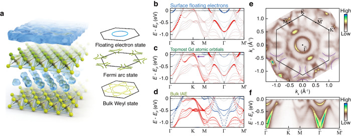
Fig. 1. Crystal structure and electronic structure of [Gd2C]2+·2e−.
a Schematic of the crystal (left panel) and electronic (right panel) structures. In the left panel, the green and black spheres represent Gd and C atoms, respectively, forming [Gd2C]2+ layers. Blue blobs between the [Gd2C]2+ layers denote bulk interstitial anionic electrons (IAEs). The floating electrons are depicted atop the crystal structure. The right panel illustrates the electronic structure corresponding to the crystal structure. The bulk of the crystal exhibits a non-trivial band topology, hosting the bulk Weyl state. The Fermi-arc state is observed on the [Gd2C]2+ surface, while the floating electron state reveals a circular Fermi surface. b–d Calculated electronic structures with contributions from electrons at the surface floating electrons (b), the topmost Gd atoms (c), and the bulk IAEs (d). Blue and red colors denote major and minor spin components, respectively. The purple arrow in (c) marks the predicted Fermi-arc dispersion. e, f Fermi surface (e) and high-symmetric line dispersions (f) obtained from ARPES measurements with 90 eV photons. The Fermi surface was symmetrized along direction. The black solid line on (e) represents the 1st Brillouin zone (BZ) boundary, and the purple dashed lines near and points guide the expected Fermi arcs.

