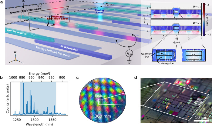
Fig. 1. Hybrid integration architecture.
a Schematics for foundry-based quantum photonics based on hybrid integrated tunable single-photon quantum emitters. Alignment between the waveguides of an InP chiplet and the silicon photonic integrated circuit (PIC) enables single photon adiabatic coupling in the resulting hybrid structure. We resonantly excite the emitters by focusing a laser beam onto the chiplet’s emitters. Applying a voltage, VSi between tuning and a ground electrode applies an electric field, represented as black lines, across the InP waveguide, thereby tuning the emission frequency of the enclosed QDs through the quantum confined Stark effect. Inset: finite element simulations of the electric field, white lines overlaid on the component Fw normal to the PIC surface, inside the InP waveguide. QDs can experience various degrees of screening due to stray charges modeled here as surface charge densities of ±σ. An additional laser beam with an energy above the bandgap of the chiplet can further affect these charge distributions, thus providing another mechanism for tuning the emission frequency of the QDs. b Representative photoluminescence spectrum from an ensemble of QDs, where the blue shading denotes the O-band, collected from photons that have been routed through the PIC. c Photograph of a 300 mm wafer on which our PIC was fabricated using a foundry process. d Closer view of a reticle from the wafer in c showing the location of our chip.

