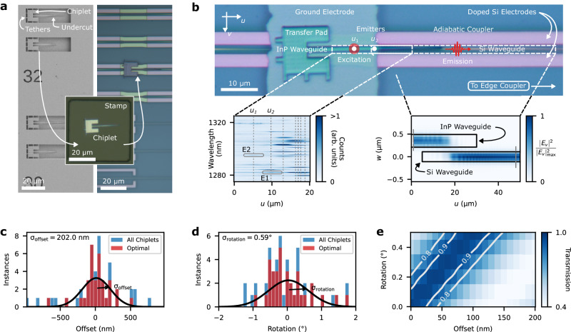
Fig. 2. Hybrid PIC Assembly.
a Scanning electron (left) and optical (right) micrographs of the suspended InP chiplets and of the hybrid photonic integrated circuit (PIC) at the transfer printing stage of its assembly, respectively. b Optical micrograph of the transferred microchiplet surrounded by the components tuning its emitters and routing single photons to the silicon-on-insulator (SOI) PIC. Left inset: photoluminescence spectra acquired while exciting emitters at various positions along the chiplet’s nanobeam. Right Inset: Finite difference time domain simulation of the InP waveguide quasi-TE mode coupling from the chiplet to the PIC, where Ev denotes the out-of-plane component of the electric field. c Relative offset and d rotation of 48 InP chiplets with respect to their underlying silicon waveguides on the PIC. The All Chiplets data set corresponds to data extracted from tapers attached to all the chiplets that were transferred onto SOI PICs. The Optimal data set only considers chiplets that did not experience any complications in their transfers due to residue underneath the chiplets. e Simulated optical transmission through the InP–silicon junction for various degrees of misalignment between the two tapers.

