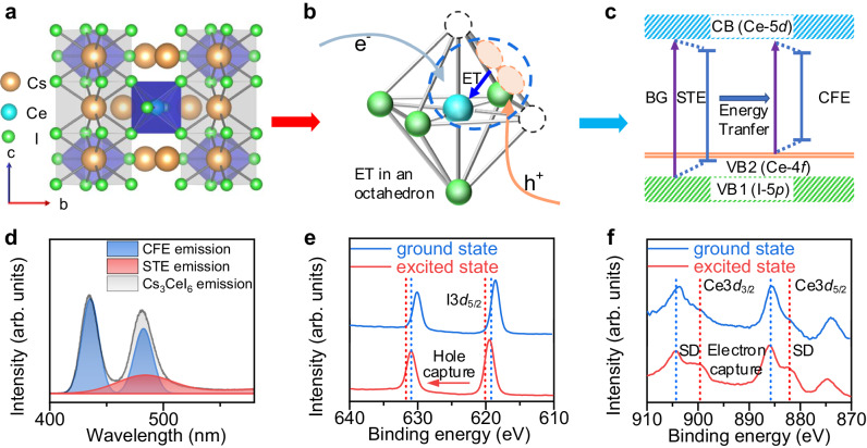
Fig. 1. Modeling and characterization of the energy transfer process in Cs3CeI6.
a Crystal structure of Cs3CeI6. b Schematic diagram of STE formation and energy transfer process. The circular part of the blue dashed line shows the formation of STE and its energy transfer to CFE. ET stands for energy transfer. c Schematic diagram of Cs3CeI6 energy band structure and two types of excitons. The electrons and holes of STE come from CB and VB1 (contributed by Ce-4f) respectively, and those of CFE come from CB and VB2 (contributed by I-5p) respectively. (BG for bandgap, STE for self-trapped exciton, CFE for Ce Frenkel exciton, CB for conduction band, and VB for valence band). d CFE, STE, and total emission spectra of Cs3CeI6 crystal in 4.2 K. e X-ray photoelectron spectroscopy of I−3d5/2 in Cs3CeI6 in the ground and excited states (in which the excited state is generated by continuous irradiation of 280 nm laser for 5 min). f X-ray photoelectron spectroscopy of Ce-3d3/2 and Ce-3d5/2 in Cs3CeI6 in the ground and excited states.

