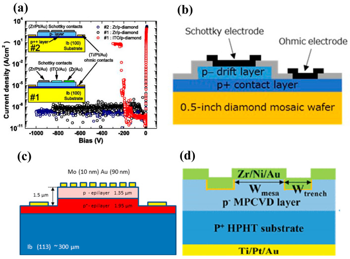
Figure 13.
Device schematic of (a) pVSBDs with p+ doping concentration of 1020 cm−3 and p- doping concentration of 1015 cm−3 [106]; (b) pVSBDs using a half-inch diamond wafer [131]; (c) pVSBDs on (113)-oriented homogeneous epitaxial boron-doped diamond substrates [130]; and (d) trench MOS barrier Schottky diodes [77].

