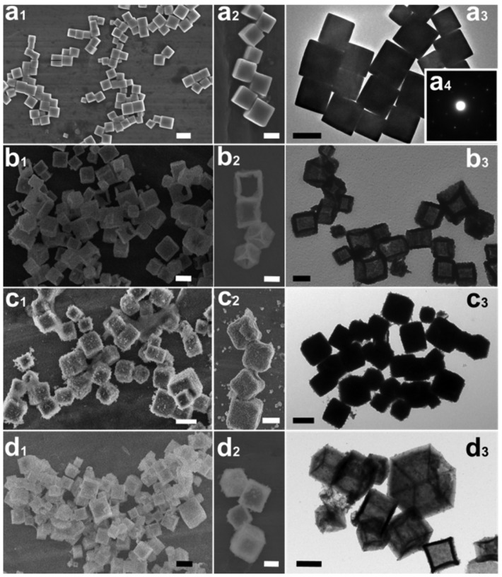
Figure 2.
The SEM (x1 and x2) and TEM (x3) images of the Cu2O cubes, composite CeO2-Cu2O (1), NiO@Cu2O (2), and CeO2–NiO–Cu2O (3). (x = a, b, c and d for Cu2O and composites 1−3, respectively) The scale bar is 800 nm in parts x1 and x3, and it is 500 nm in part x2. Figure reproduced from ref. [89]. (a1,a2) The SEM images of Cu2O cubes; (a3) The TEM images of Cu2O cubes; (a4) The SAED pattern of Cu2O cubes; (b1,b2) The SEM images of composite CeO2-Cu2O; (b3) The TEM images of composite CeO2-Cu2O; (c1,c2) The SEM images of composite NiO@Cu2O; (c3) The TEM images of composite NiO@Cu2O; (d1,d2) The SEM images of composite CeO2–NiO–Cu2O; (d3) The TEM images of composite CeO2–NiO–Cu2O.

