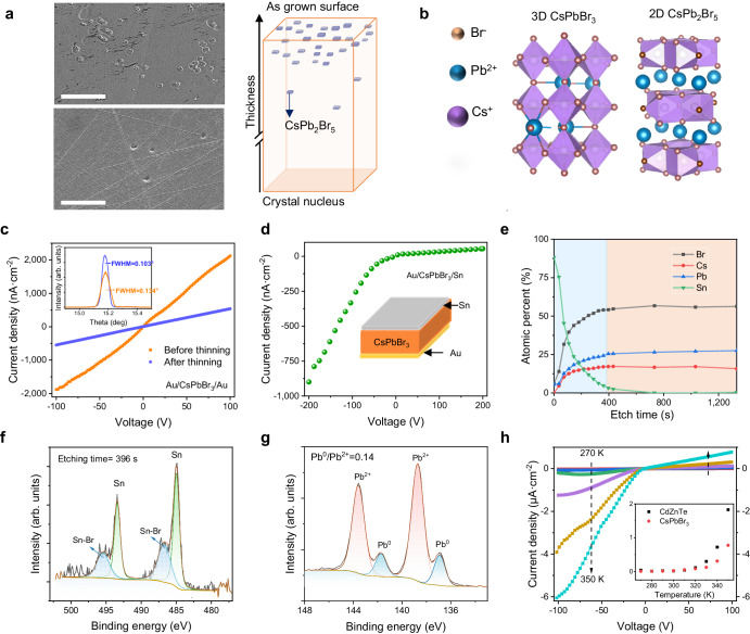
Fig. 2. Device performance of planar CsPbBr3 devices.
a The CsPb2Br5 phase defects at different crystal thicknesses. The scale bars in white color are 20 μm. b The structure of CsPbBr3 and CsPb2Br5. c J-V characteristics for the planar Au/CsPbBr3/Au device (the inset is X-ray rocking curves of the CsPbBr3 single crystal) before and after thinning (d = 1 mm). d J-V characteristics for the Au/CsPbBr3/Sn device. e Atomic percentage vs. etching time of each element of Sn/CsPbBr3. f X-ray photoelectron spectroscopy (XPS) with an etching time of 396 s. g Pb 4 f XPS spectra at the interface. h Temperature dependence response of the Au/CsPbBr3/Sn device from 270 K – 350 K. (The inset is the comparison of leakage current between CsPbBr3 and CdZnTe at different temperatures with the same electric field of 1000 V cm−1).

