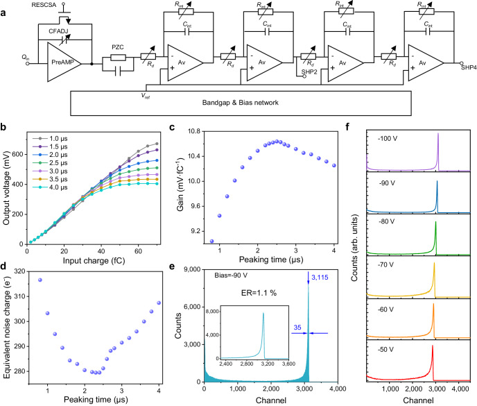
Fig. 5. Device performance from an optimized the electronics design.
a Block diagram of one channel in the readout circuit with a built-in bandgap and bias circuit. Qin is input charge. PreAMP is a preamplifier. RESCSA is the bias voltage for controlling the feedback transistor. CFADJ is the voltage for adjusting the feedback capacitor. PZC is pole-zero cancellation circuit. Av is the operational amplifier. SHP is the output of each stage of the slow shaper. Rint is an integral resistor, Cint is an integral capacitor, and Rd is a differential resistor. Vref is the reference voltage. b The amplitude output voltage of shaper Vout versus input charge Qin at different peaking time. c Measured conversion gain versus peaking time. d Measured ENC versus peaking time. e α particles spectra with energy resolution of 1.1% with thickness is 1 mm. f α particles spectra acquired by the Au/CsPbBr3/Sn detector with different applied voltage (d = 1 mm).

