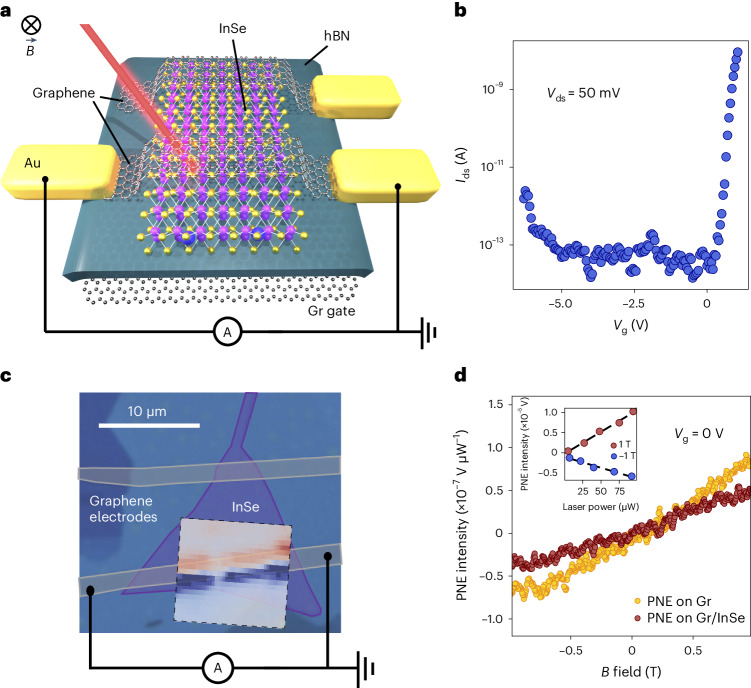
Fig. 1. Device schematics and basic characterization.
a, Device schematic representing a fully encapsulated few-layer InSe channel, with graphene electrodes. One of the electrodes is contacted on both sides with gold contacts to perform measurements of graphene, affected by InSe. The scanning photocurrent maps are performed at 100 mK, with 50 µW laser power and an out-of-plane magnetic field of 1 T, unless specified otherwise. b, Electron transport characteristics of a typical few-layer InSe device, in this case 3L InSe, performed at a low temperature under 50 mV of bias. c, Optical micrograph of a 3L InSe device with graphene electrodes. An examplary measurement of the photo-Nernst effect at 1 T measured on graphene is shown overlapped with the region of interest. d, Linear magnetic-field dependence of the Nernst effect when the illumination is on graphene alone (dark yellow) and Gr/InSe (dark red). The inset shows the power dependence of the Nernst effect on Gr and sign change for an opposite magnetic field, confirming the origin of the effect as the photoinduced Nernst effect (PNE).

