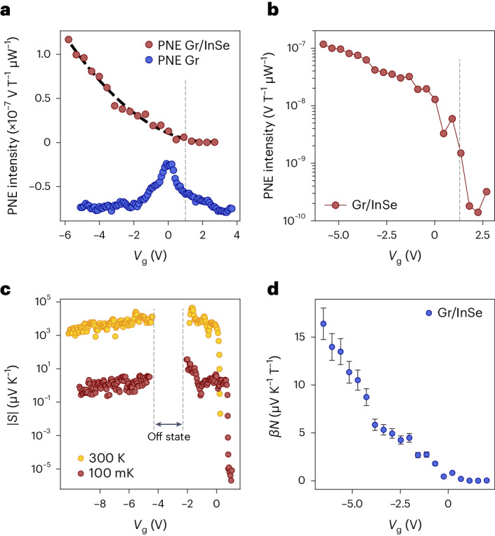
Fig. 2. Photo-Nernst effect and thermoelectric performance.

a, Nernst effect intensity normalized by laser power measured on the 3L InSe/Gr heterostructure (dark red) as a function of gate voltage. The Nernst effect of bare graphene is shown as a comparison (blue), and is offset for clarity. b, Nernst effect intensity of the heterostructure plotted in the logarithmic scale to highlight the sizable on/off ratio. The effect can be switched on and off by changing the carrier density within our device. The grey dashed lines represent the onset of n-type conduction, analogous to a. c, Seebeck coefficient calculated through the Mott relations (Supplementary Note 10) as a function of gate voltage, shown for 300 K (yellow) and 100 mK (red). The vertical grey dashed lines represent the off state of the device, where the Seebeck coefficient cannot be defined due to the high resistance of the device, which becomes comparable with the input impedance of the instrument38. d, Gate-tunable Nernst coefficient in the Gr/InSe heterostructure. The plot represents a lower bound for the real value, due to β. The error bar reflects the error present in the determination of temperature (Supplementary Note 3).
