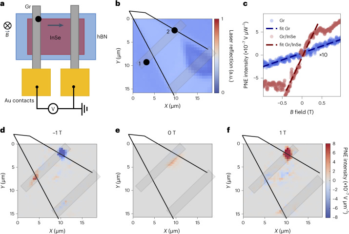
Fig. 3. Scanning photovoltage map of the Nernst effect across an InSe channel.
a, Device schematic showing the illumination of the Gr/5L-InSe heterostructure and electrical detection across the InSe channel. b, Laser reflectance map of the region of interest measured simultaneously with the scanning photovoltage map. This measurement allows us to correlate the position of the laser with the observed signal. The positions chosen to record the Nernst effect signal on graphene and on the Gr/InSe heterostructure are labelled as positions 1 and 2, respectively. c, Nernst effect signal recorded by varying the magnetic field and under 50 µW of laser illumination and Vg = 0 V in positions 1 and 2, shining light on the graphene electrode and on the heterostructure, respectively. The bare graphene signal is shown in blue, multiplied by 10 to better highlight the difference in slope between the two curves. The measurements are performed without any applied bias as it would obscure the Nernst effect, inducing other photovoltage mechanisms in the picture. d, Scanning photovoltage map showing the measured photovoltage across the full device at an applied out-of-plane electric field of –1 T. Here the temperature gradient is along the direction of the graphene electrode, orthogonal to the magnetic field and the measured potential. e,f, Scanning photovoltage maps shown for 0 T (e) and 1 T (f). Rectangles in b,d–f represent graphene contacts.

