Figure 3.
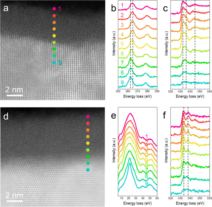
EELS line profiles of surface oxides on Nb and Ta. a, HAADF-STEM micrograph of the NbOx-Nb interface of the bare Nb thin film. Colored spots denote the positions in which EEL spectra are taken. b, c, Corresponding spatially resolved EEL spectra showing ELNESs of Nb M23 edge and O K edge. d, HAADF-STEM micrograph of the TaOx-Ta interface of Ta-capped Nb thin film. Colored spots denote the positions in which EEL spectra are acquired. e, f, Corresponding spatially resolved EEL spectra showing ELNESs of Ta O23 edge and O K edge. The distance between adjacent spots is 0.83 nm.

