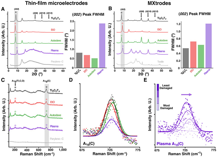
Figure 3. Raman and XRD analysis of pristine and sterilized devices.
(A, B) Left: XRD patterns including pristine control and Parylene-C or textile backgrounds. Right: FWHM of the (002) peak for (A) thin-film devices and (B) MXtrodes (n = 2 for each condition). (C) Raman spectra including pristine controls and Parylene-C background for thin-film devices. (n = 2 samples for each condition). (D) Normalized Gaussian-fitted A1g(C) peak for thin-film devices. (E) Right-shifting Normalized Gaussian-fitted A1g(C) peak for increasingly visually damaged thin-film samples after H2O2 gas plasma sterilization.

