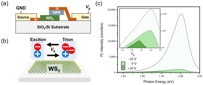
Figure 7.
(a) Schematic describing the top-gated device structure. The top graphene layer acts as a gate electrode to apply electrostatic doping onto the WS2 monolayer, while the bottom graphene is electrically ground. (b) Gate voltage-dependent modulation of PL in the WS2 monolayer enabled by adjusting the exciton and trion density. (c) PL spectra of the WS2 monolayer with gate voltages of Vg = −20 V, 0 V, and +20 V measured at an incident power of 1 W/cm2.

