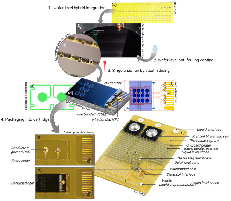
Figure 2.
(a,b) Wafer level flip-chip bonding of PDs. GaAs PD dies are individually transferred from a carrier and bonded to a wafer by laser-assisted local reflow soldering (right). (c) Close-up on multiple VCSELs, PD arrays, and NTCs populated on a wafer. (d) Completely assembled, wire-bonded and stealth-diced hybrid PIC (with ‘large’ spirals), VCSEL, PD arrays, and NTC. (e,f) Design of the hybrid PIC. (f) Front side with photonic waveguide circuitry (red), Cr-Au metallization (yellow), etched sensing windows (blue) with ‘small’ spirals, and microfluidic flow channel (purple). (e) Backside with Ta-Pt resistive heater. (g,h) Close-up of the PIC cavity of the PCB. (a) After dispensing electrically conductive glue; (b) after placement and encapsulation of the hybrid PIC. (i) Photograph of the microfluidic cartridge. The labelled features of the cartridge are discussed in the text.

