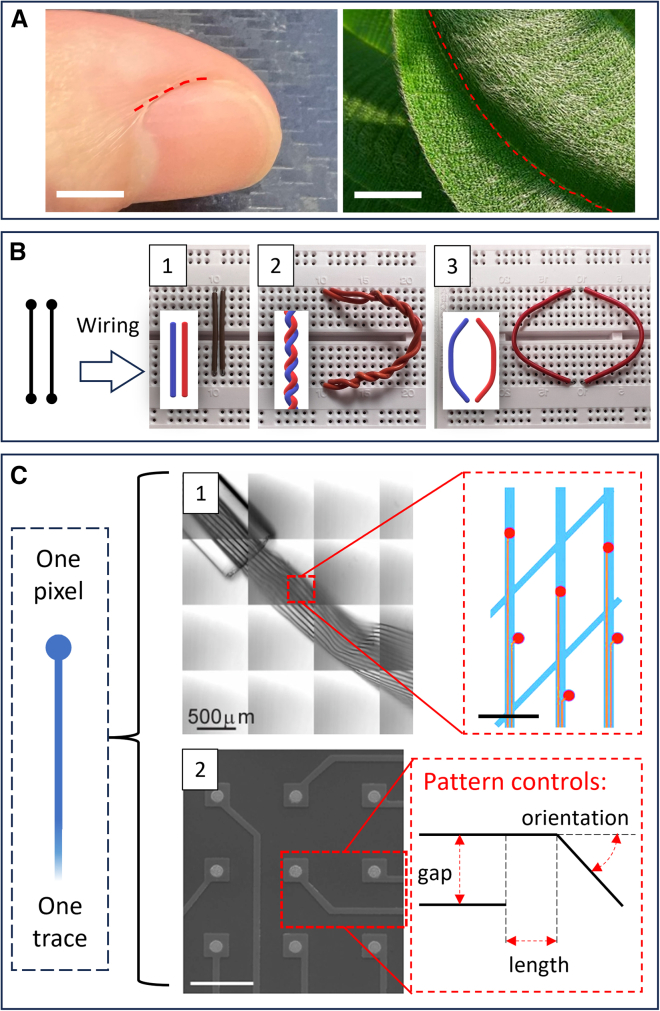
Figure 8.
Adaptability in bioelectronic fiber building blocks
(A) Example geometries on biological surfaces that may challenge reliable bioelectronic fiber deployment, demanding deployment adaptability. Left: sharp edge at the side of fingernails. Right: the edge between overlapping leaves as well as trichomes on leaf surfaces. Original photo adapted with permission.83 Copyright 2007, Clyde Robinson. Scale bars, 5 mm.
(B) Different entanglement configurations for a pair of wires with identical connection logic (neighboring parallel fibers, left). The physical jumper wires in the photos connect the top and bottom sockets of two adjacent columns; the wires are structurally mechanically comparable to individually handleable bioelectronic fibers. (1) Simple parallel fibers as the basic configuration. (2) The “twisted pair” configuration that reduces inductive noise between wires. (3) Using increased distance between wires for reducing capacitive noise.84 (Insets show generalized wire entanglement schematics.).
(C) Two structurally different bioelectronic pixel device examples with the same “one pixel, one trace” circuit topology that may support modular adaptability; each trace and pixel can be designed to be individually manipulable and replaceable using bioelectronic fiber building blocks. (1) Microscopy photo of a mesh-like bioelectronic device made with bundled bioelectronic fibers (left); pixel conductor traces (red lines) each connect to individual pixels (red circles) fabricated on the mesh filaments (blue). Scale bar, 50 μm (right). Reproduced with permission.85 Copyright 2017, Fu et al. (2) Example SEM photo of a planar bioelectrode pixel array with identical topology as in (1). Scale bar, 100 μm (left).86 The schematic shows key pattern control factors for arranging mutually separated pixel traces, which is also a deployment adaptability requirement for using fiber building blocks to construct pixel structures (right). Left: adapted with permission.86 Copyright 2020, Yoo et al.

