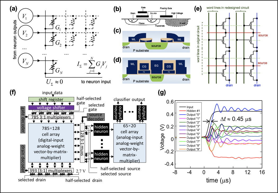
Figure 1.
(a) Generic scheme of analog vector-by-matrix multiplication in a crossbar circuit with adjustable crosspoint devices. For clarity, the output signal is shown for just one column of the array. (b-d) Schematic cross-sections of (b) synaptic transistor, and (c) ESF1 and (d) ESF3 supercells. ESF stands for Embedded SuperFlash NOR flash memory technology. Such technology is based on array of supercells, with each supercell hosting two split-gate floating-gate transistors. (e) 2×2 fragment of the ESF1 supercell array, highlighting the routing of word lines in the original NOR flash memory (dashed green lines) and in the array modified for analog applications (solid green lines). (f) Network for classification of MNIST benchmark images, with 105+ FG cells, implemented in 180-nm technology, and (g) the typical dynamics of the network’s input signal, the output of a sample hidden-layer neuron, and all network’s outputs, after an abrupt turn-on of the voltage shifter’s power supply [6].

