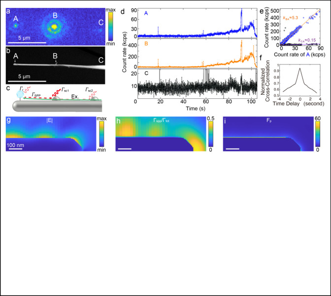
Figure 2.
Observation of the nanoparticle trapping by the plasmonic probe. (a) Representative wide-field PL image extracted from video footage showcasing an FND trapped at site A on a AgNW probe. Particles at sites B and C on the AgNW surface facilitate the coupling of SPPs into free space. (b) The SEM image validates the presence of the nanostructures at the specified locations. (c) Schematic representation of the energy transfer pathways within the FND-AgNW assembly. (d) Temporal fluorescence intensity profiles for PL emission from the three distinct locations. (e) Analysis of PL intensity correlations between the different spots. (f) Normalized cross-correlation of events from sites A and B. (g) Distribution of the electric field of the HE1 mode SPP introduced into the AgNW from the left port. (h) Visualization of SPP mode coupling efficiency from a quantum emitter, derived from the positional mapping of an electrical dipole emitter. (i) Spatial representation of the Purcell factor (Fp) for a dipole emitter at varying proximities.

