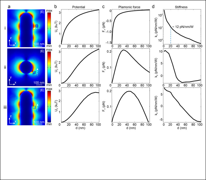
Figure 4.
Computational assessment of trapping potentials: (a) Distribution profiles of the electric field for the HE1 mode across various cross-sectional planes. (b) Mapping of optical trapping potentials along different trajectories, as identified in panel (a). It is calculated by integrating the optical trapping forces (Fx, Fy, Fz) in (c), which are derived from Maxwell’s stress tensor. (d) Associated potential well stiffness (kx, ky, kz) exerted on the quantum dot, ascertained from the calculated force distributions.

