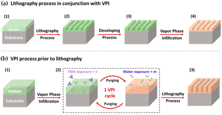
Figure 6.
(a) Workflow for patterning integrated with VPI: (1) applying resist onto a Si substrate using spin-coating, (2) exposing the pattern using e-beam or EUV lithography, (3) development step, and (4) SIS infiltration. (b) Workflow for VPI before lithography: (1) applying resist onto the substrate using spin-coating, (2) infiltrating with , and (3) pattern exposure using e-beam or EUV lithography [30].

