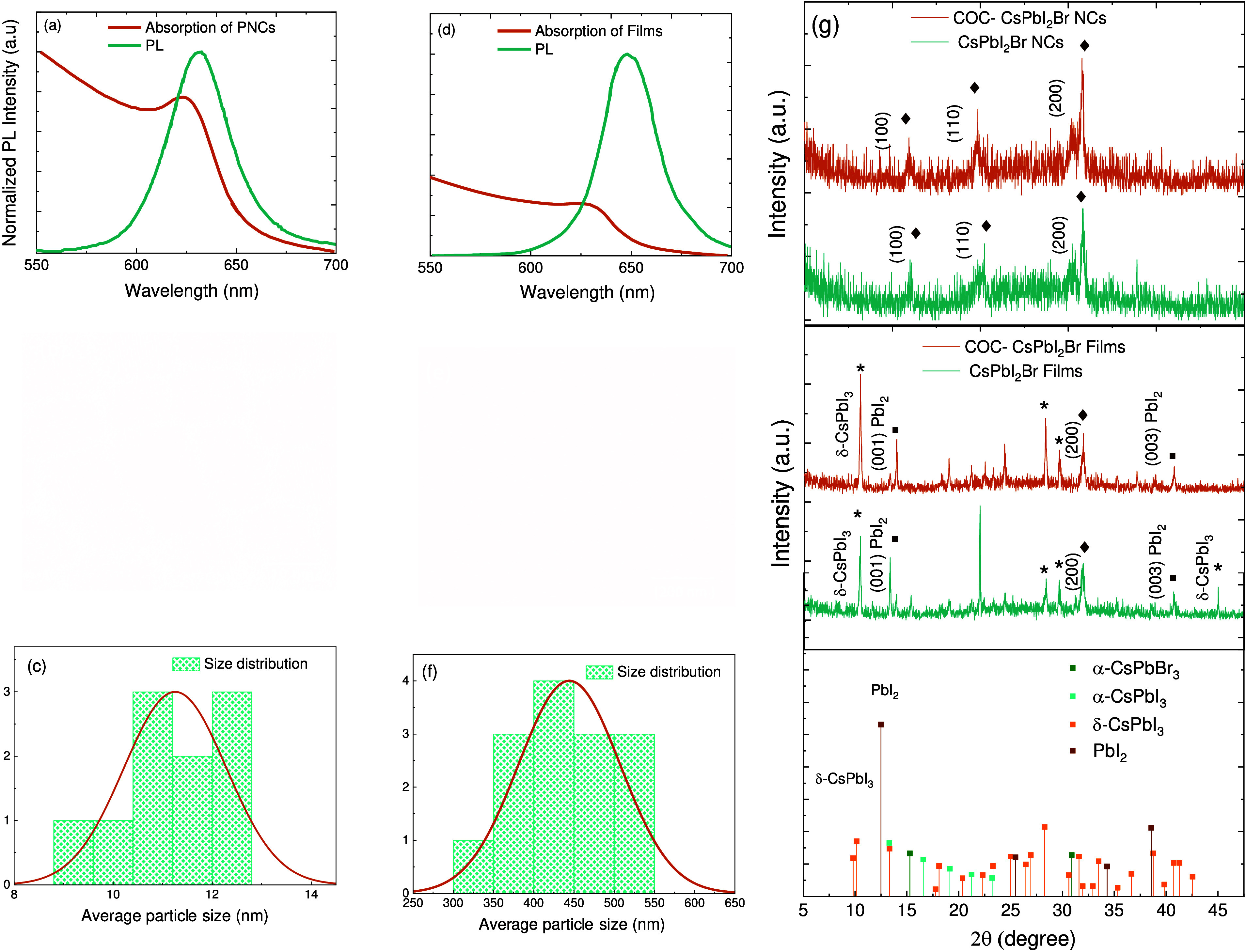
Figure 1.

(a) Ultraviolet–visible (UV–vis) absorption and photoluminescence (PL) spectra of CsPbI2Br PNCs obtained under air conditions. (b) Transmission electron microscope (TEM) images of CsPbI2Br PNCs. (c) Size distribution of CsPbI2Br PNCs (11.30 nm in size) from TEM images. (d) UV–vis absorption (PL) spectra of CsPbI2Br thin films obtained under air conditions. (e) SEM images of CsPbI2Br thin films. (f) Grain size distribution with ∼450 nm CsPbI2Br thin films. (g) XRD patterns of the CsPbI2Br PNCs and film counterparts before and after encapsulation upon 405 nm illumination with an average power density of 3180 W cm–2.
