Abstract
An original metal catalyzed CVD methodology assisted by hydrogen plasma for the direct deposition of few-layer graphene on a substrate is presented. Graphene is grown at 900 °C directly on the surface of the substrate of technological interest by carbon diffusion through a nickel film by using methane (CH4) as the carbon precursor. Hydrogen atoms in the H2-plasma downstream are used to promote the solubilization of carbon atoms in Ni, thus favouring the growth of graphene at the Ni/substrate interface. Structural and transport properties of the as-grown multilayer graphene films on SiO2/Si and quartz substrates are provided. We demonstrate the peculiarity of this approach for controlling the thickness and transport properties of as-grown graphene films using process-step times. Finally, the potential of the proposed methodology for the bottom-up direct growth of patterned graphene is demonstrated.
Hydrogen radicals promote carbon diffusion through nickel films and graphene growth on the substrate surface.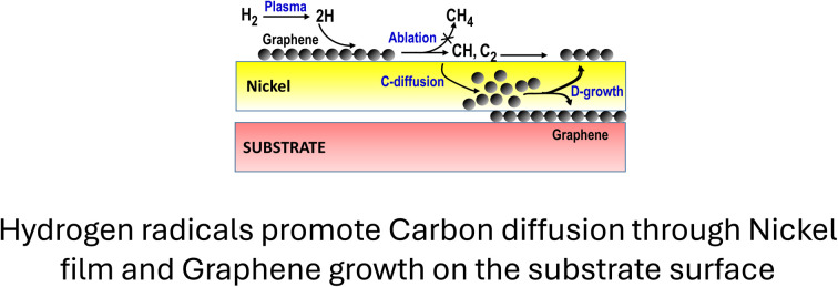
Introduction
Metal catalyzed CVD growth on Cu and Ni foil is a well-established methodology for fabricating large area single- and few-layer graphene with high structural quality and transport properties.1–6 However, graphene implementation in devices typically involves deterioration of its material structural integrity as well as polymer contaminations following the transfer process from the metal foil onto the desired substrate.7 Moreover, graphene transfer has limits on substrates with important roughness and low surface wettability as well as scalability and cost- and time-effectiveness issues.
Significant efforts are currently being made to explore new growth methodologies to obtain graphene directly on semiconductor and dielectric substrates.8,9 Graphene transfer-free deposition approaches can be mainly classified into metal-catalyst-free10,11 and catalyzed-transfer-free methodologies.12–16
Metal-catalyst-free methodologies need high temperature (1400–1600 °C) to overcome reaction energy barriers for the decomposition of gaseous precursors and activation of graphene growth. Typically, reactors with specific cold wall design are required to confine chemical processes on the substrate surface11 and the range of suitable substrates is confined to high melting point materials (such as sapphire). The temperature for the activation of the graphene growth process can be reduced by tuning the surface chemistry of the substrates. Chen et al.17 obtained the direct growth of graphene at 1100 °C on SiO2/Si and quartz substrates by exploiting O2 plasma pretreatment of the substrates. They demonstrated the role of oxygen functionalities on the surface for enhancing the adsorption of hydrocarbon radicals and promoting C–C coupling to nucleate graphene grains. Other metal-catalyst-free methodologies exploit plasma enhanced CVD processes to obtain carbon precursor decomposition at temperature as low as 500 °C.18 However, the quality (defectivity, thickness homogeneity, grain sizes, etc.) of PE-CVD graphene was not comparable to that of the material obtained by thermally activated growth processes.
Catalyzed-transfer-free deposition methodologies use evaporated or sputtered films of transition metal catalysts (typically, Cu or Ni) to assist the formation of graphene layers at the metal-substrate interface. The following wet etching of the metal film uncovers the graphene directly deposited on the substrate, thus eliminating the need for a transfer step. Catalyzed-transfer-free graphene growth can use an amorphous carbon layer as a carbon source or, more in general, a carbon-based layer covered by a Ni film to promote carbon recrystallization as graphene by annealing.19 The high saturate solubility of carbon in Ni (∼1.3% at 1000 °C13) allows carbon diffusion from the top of the metal film toward the metal/substrate interface where dissolved atoms can precipitate and segregate as graphene layers.14 Baraton et al. tested a dual step methodology consisting of plasma-enhanced CVD deposition at 450 °C of a highly defective graphene film on top of a Ni film, followed by an annealing step at 900 °C.15,16 The authors highlighted how understanding and controlling the phenomena allowing the carbon species at the surface of the catalyst to diffuse to the nickel/silicon oxide interface is crucial to improve graphene segregation on the substrate rather than the formation of graphite pillars into the nickel layer. Moreover, the carbon solubilization process can be limited or completely avoided by the passivation of the catalyst due to the formation of stable graphene layers on the Ni film surface.20
In the present work, we investigate the growth of graphene with the catalytic CVD methodology on nickel, with the aim of maximizing direct growth on the substrate. The main question we want to answer is the following: is it possible to implement carbon diffusion and thus carbon solubilization in nickel in such a way as to produce significant growth at the nickel–substrate interface? We report the growth of multilayer graphene on SiO2/Si and quartz substrates by the Ni catalyzed CVD process assisted by H2 plasma. High quality and full coverage of the graphene layers on the surface of substrates are confirmed by Raman spectroscopy and electrical measurements.
Materials and methods
Sample preparation
A Ni film has been deposited on SiO2/Si and quartz substrates using a magnetron sputtering system (HEX Series Korvus Technologies) operating at 20 W at 3.0 × 10⁻³ mbar (Ar ambient) at room temperature. Metal film thickness has been controlled using a quartz crystal microbalance.
After Ni film sputtering the samples have been immediately transferred and processed in a quartz reactor with an external furnace to limit the metal oxidation kinetics. Samples have been annealed (heating rate of 14 °C min−1) in hydrogen ambient at 2.6 mbar, 900 °C, for 10 min. Then, a H2 plasma pretreatment with a remote plasma source has been carried out at 900° for 4 min in order to remove native oxide on the Ni film.
Graphene growth
CVD graphene growth is carried out at 900 °C and 5 mbar in CH4/H2 (ΦCH4 = 40 sccm; ΦH2 = 40 sccm) ambient. H2 plasma is generated in the remote upstream part of the CVD reactor through a capacitive coupled radiofrequency (13 MHz) power supply (power 100 watt and a H2 pressure of 2.5 mbar). The electrodes are 40 cm away from the center of the furnace to ensure that the energetic hydrogen ions (H+, H2+, …) do not reach the CVD growth zone leaving only neutral H-atoms. The H2 plasma assisted growth is carried out in a preliminary CVD step of 30 min, followed by several cycles of H2 plasma and CVD steps of respectively 4 min and 10 min.
After the growth phase, the furnace is moved from the growth-zone to realize the rapid cooling of the samples. A wet etching treatment in HCl : HNO3 : H20 (1 : 2 : 60) for 60 min is used for uncovering graphene grown on the substrate surface from the Ni film and graphene on-top layers.
Characterization
Raman spectra of graphene were recorded with a LabRam HR (Horiba JY) system. All spectra were measured at room temperature and captured using 100× objective lens magnification with a focusing laser spot less than 1 μm in diameter. Measurements of graphene on the Ni film were carried out with 473 nm laser light to reduce background Ni luminescence in spectra. 532 nm laser light was used for measuring graphene on SiO2/Si and quartz substrates. The laser powers of both 473 and 532 nm laser sources were kept at 1.0 mW to avoid the laser-induced heating effect. The sheet resistance measurements were carried out with a Keithley 2400 Source Meter, using a home-built 4-probe Van der Pauw configuration system.
Results and discussion
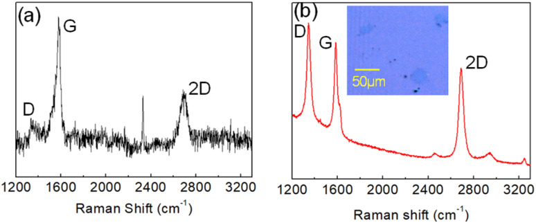
Unlike Cu-catalyzed CVD growth, in which the low solubility of carbon in copper confines the growth of graphene on its surface, the Ni-catalyst presents a high solubility which implies an important contribution to the growth of graphene by diffused carbon in the nickel bulk. Fig. 1a shows the Raman spectrum of graphene grown by the CVD methodology (60 min at 900 °C) on the surface of a 50 nm Ni film supported by a SiO2/Si substrate. As expected, the ratio between the intensities of the G peak and 2D peaks (respectively at 1585 cm−1 and 2700 cm−1) attests to the growth of the multilayer graphene film as expected when Ni is used as the metal catalyst.
Fig. 1. (a) Raman spectrum (473 nm laser source) of CVD graphene grown on a 50 nm Ni film supported by a SIO2/Si substrate. (b) Raman spectrum (532 nm laser source) of graphene islands on the SiO2/Si substrate after removal of the Ni film using etchant solution. The optical image of graphene islands on the SiO2/Si substrate is shown in the inset.
The main thermally activated chemical processes occurring
| CH4(g) ↔ CH4(ads) → CH(ads), C2(ads) + H2(g) | 1 |
| CH(ads), C2(ads) → C-sp2(graphene) + H2(g) | 2 |
| CH(ads), C2(ads) → C(bulk) + H2(g) → C-sp2(graphene) | 3 |
during the CVD growth on the top surface of the Ni thin film can be summarized as: (1) the adsorption/desorption of gaseous methane molecules (CH4(g)) on free active sites on the Ni top surface, followed by the catalyzed dehydrogenation and production of active species CH and C2; (2) the graphene growth; (3) the carbon solubilization in the metal film (C(bulk)) that contributes to the growth by diffusion.
Reactions in eqn (2) and (3) are competitive processes whose kinetics stops when graphene (from reaction eqn (2)) covers all Ni surface and, hence, no more active sites are available for CH4 adsorption.21 However, in contrast to CVD growth on the Cu catalyst, the higher carbon saturated solubility in Ni (∼1.3% atomic at 1000 °C (ref. 22)) promotes graphene growth also by C-diffusion (eqn (3)) during both the metal annealing step and the cooling step. Indeed, a decrease in temperature also reflects a decrease in carbon solubility, thus promoting the solubilized carbon outdiffusion and precipitation as supplementary graphene layers (reaction eqn (3)).
Thus, in the case of Ni films of tens of nanometers, carbon diffusion through film thickness can promote reaction in eqn (3) both on the metal surface as well as at the metal/substrate interface. Indeed, after removal of the Ni film by wet etching, optical microscopy and Raman spectroscopy reveal the presence of graphene islands formed directly on the SiO2/Si surface (see Fig. 1b). The Raman spectrum of these graphene islands (Fig. 1b) strongly differs from the Raman spectrum of the graphene film grown on the Ni surface (Fig. 1a), thus indicating different structural properties. In contrast to the multilayer nature of CVD graphene grown on Ni, the I2D/IG ratio of Raman peaks as well as the narrower FWHM of the 2D peak of graphene islands are characteristic of a single layer material. Moreover, graphene islands present an intense D peak at 1343 cm−1 that is a measure of defectivity in the crystalline grain.
As reported in the introduction paragraph, the low material quality as well as the low coverage of graphene segregated at the metal/substrate interface derives from the low amount of C(bulk) diffusing and reaching the SiO2/Si substrate. Specifically, carbon flux in Ni is driven by the presence of a concentration gradient through the thickness of the metal film, according to Fick's laws.12 During annealing, CHx(ads) dissolving on top of the Ni film would provide a continuous C(bulk) feeding (reaction n. 3) able to sustain a concentration imbalance through the metal film thickness and promote carbon diffusion toward the Ni/substrate. However, the processes involved in the metal catalyzed CVD growth of graphene are self-limiting processes.23 When the Ni surface is completely passivated due to the formation of stable graphene layers (from reaction eqn (2)), no more active sites are available for the catalytic decomposition of gaseous carbon precursors (reaction eqn (1)).20 Thus, no more CHx and C2 active species are generated and solubilized in the Ni bulk also for longer exposure time to the gaseous precursor.
In order to increase the C(bulk) feeding in coverage metal film we use hydrogen atoms for exploiting these on-top passivating graphene layers as supplementary solid sources of carbon active species (reaction eqn (4)) which can solubilize in the Ni bulk.
| C-sp2graphene + H → CHx(ads), C2 + H2 | 4 |
According to reaction eqn (3), the generated CHx and C2 active species can be solubilized in Ni so as to increase the concentration gradient in the metal bulk and, hence, the further growth by diffusion (D-growth) at the nickel–substrate interface.
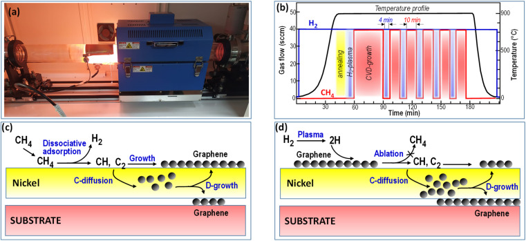
The method we have optimized to achieve this objective is based on alternating CVD-growth and H2 plasma stages using exposure to a CH4–H2 mixture and H2-plasma intermittently. Fig. 2 schematizes the approach we used to develop the experiments. During the CVD step dissociative chemisorption of CH4 molecules (reaction eqn (1)) promotes both the graphene growth on the Ni surface (reaction eqn (2)) and the carbon solubilization in the metal film (reaction eqn (3)) according to the scheme in Fig. 2c.
Fig. 2. Direct graphene growth on the substrate by alternating CVD-growth steps with H2-plasma processes. (a) Image of the CVD reactor during the H2 plasma stage, (b) process–time diagram showing the individual processes of annealing, H2-plasma for substrate cleaning, and the initial CVD-growth (red glow) followed by the intermittent H2-plasma (blue glow) to favour the diffusion growth (D-growth) on the substrate. (c and d) Schematization of the processes that occur in (c) the CVD growth stage and (d) the H2-plasma stage. The emphasis is on the role of hydrogen atoms in promoting the ablation of the graphene to CH and C2 radicals, their solubilisation in the nickel bulk and the subsequent graphene growth by diffusion (D-growth) at the nickel–substrate interface.
During the H2 plasma step, hydrogenation of graphene layers formed during the CVD step (reaction eqn (4)) helps their dissolution in Ni and, at the same time, regenerate active sites for methane chemisorption during the subsequent CVD step.
The interaction of H atoms with graphene has been widely investigated in the literature as a means for tuning graphene physical properties24 as well as for the material patterning by chemical etching.25 Specifically, the last process has been experimentally demonstrated to be avoided when the hydrogen/graphene interaction occurs at temperature above 800 °C.25–27 In this temperature range, incident H atoms on hydrogenated graphene promote desorption of H2 molecules by a recombination reaction rather than CHx etching as CH4 molecules.27
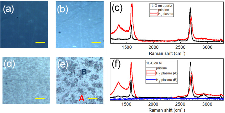
In the proposed graphene growth methodology, the H2 plasma treatment is carried out at 900 °C (that is the same temperature used for the CVD step) to minimize the carbon etching as methane.25–27 We have tested this H2 plasma treatment on single layer CVD graphene transferred on quartz and Ni substrates. The Raman data are summarized in Fig. 3. Optical images of the CVD graphene film on quartz (Fig. 3a and b) before and after plasma treatment show no substantial changes in graphene coverage which is interrupted only by cracks deriving from the graphene transfer procedure. This attests to the negligible contribution of the chemical etching process at high hydrogenation temperature. Graphene hydrogenation as well as the formation of an amorphous phase is confirmed by, respectively (see Fig. 3c), the appearance of the D peak at around 1350 cm−1 and the formation of the characteristic broad Raman features of amorphous carbon at around 1510 cm−1.28,29
Fig. 3. Optical images and Raman spectra of single layer CVD graphene on quartz (a–c) and on the Ni film (d–f) before and after remote H2 plasma treatment at 900 °C. Red and blue spectra in (f) are representative of the Raman measurements acquired in the light (A) and dark areas (B) observed on the optical image of the Ni sample after plasma treatment (e).
On the other side, optical images of the monolayer CVD graphene film on Ni (Fig. 3d and e) show a change in the Ni surface morphology which is characterized by regions with different optical contrasts. Raman analysis (Fig. 3f) reveals the characteristic peaks of hydrogenated graphene (red line) only when the laser beam is focused on the light areas (A) of the samples while no graphene (blue line) can be detected on the dark areas (B). The carbon chemical etching using H atoms being negligible at 900 °C, the observed decrease in graphene coverage demonstrates the effectiveness of H atom treatment at high temperature for promoting graphene dissolution in Ni.
In order to provide a continuous and controlled supply of carbon in Ni (i.e. to promote its diffusion toward the Ni/substrate interface and, hence, segregation as graphene), we have alternated subsequent steps of catalytic decomposition of CH4 (the CVD process) and treatment with hydrogen atoms (H2 plasma) both at 900 °C. This CVD/H2 plasma cyclic methodology has been tested on both SiO2/Si and quartz substrates both covered by 50 nm of Ni film.
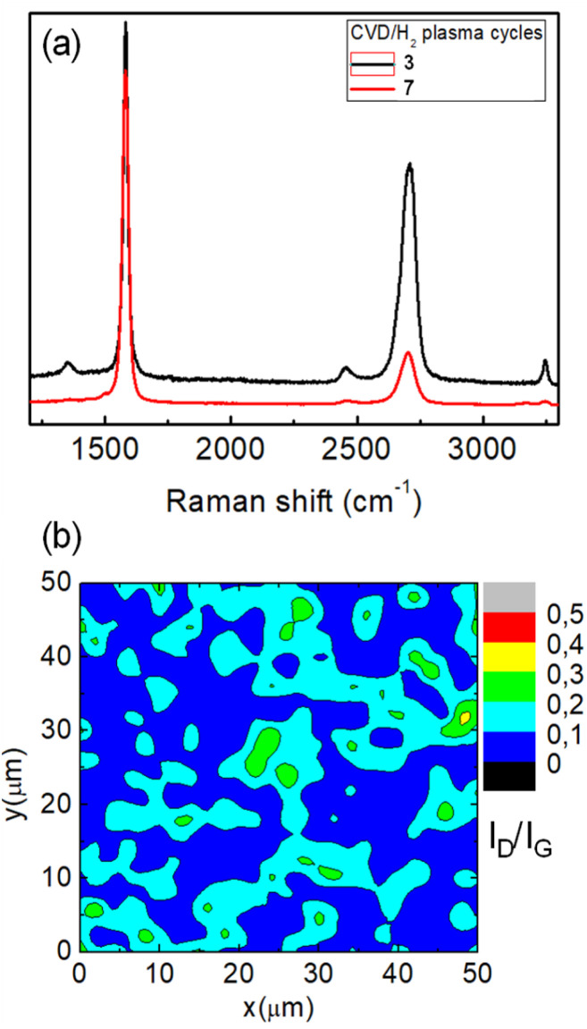
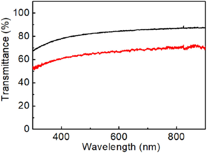
Fig. 4a shows the Raman spectra of graphene directly grown on the SiO2/Si substrate after 3 (black spectrum) and 7 cycles of CVD/H2 plasma which correspond to a total exposure time to CH4 of 60 and 100 min, respectively. After the wet etching of the Ni film, Raman measurements reveal that this methodology allows the deposition of a continuous graphene film over the entire substrate surface. Moreover, in contrast with the results reported in Fig. 1 on “conventional” CVD growth, graphene films deposited at the metal/substrate interface provide a Raman spectrum with a negligible D peak. Specifically, the Raman map in Fig. 4b reports the ratio between the intensities of D and G peaks for the graphene film grown by 3 CVD/H2 plasma steps. An average ID/IG ratio of 0.1 with a standard deviation of 0.06 results from Raman measurements over an area of 50 × 50 μm2, thus attesting to the high structural quality of the as-grown graphene. Values of I2D/IG of 0.6 and 0.2 have been estimated for, respectively, graphene grown in 3 and 7 CVD/H2 plasma cycles. These values, together with a FWHM of around 70 cm−1, are characteristics of multilayer turbostratic graphene. According to transmittance spectra reported in Fig. 5, we have estimated an equivalent thickness of, respectively, 7 layers (transmittance value of 84% at 550 nm) deposited with 3 CVD/H2 plasma cycles and 15 layers (66% at 550 nm) for 7 cycles (approximately 2–3 graphene layers deposited for each CVD/H2 cycle).
Fig. 4. (a) Raman spectra of graphene directly grown on the SiO2/Si substrate after 3 (black spectrum) and 7 cycles of CVD/H2 plasma. (b) Raman maps reporting the ratio between the intensities of D and G peaks in the Raman spectra of graphene grown in 3 CVD/H2 plasma cycles.
Fig. 5. Transmittance spectra of graphene directly grown on thw quartz substrate after 3 (black spectrum) and 7 cycles (red spectrum) of CVD/H2 plasma.
A sheet resistance, Rs, value of 130 Ω sq−1 has been measured for the 7-layer graphene. This can be correlated with an equivalent Rs in the order of 900 Ω sq−1 for each graphene layer. The last value is comparable with the Rs typically measured for single layer graphene grown by the CVD methodology. For the 15-layer sample, a Rs value of 100 Ω sq−1 is measured.
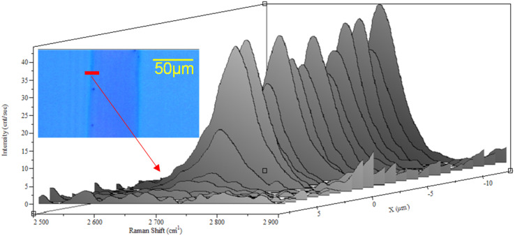
Due to the fact that graphene formation is initiated by the catalyst, we have also tested the possibility of using the proposed direct growth methodology for the localized growth of graphene on the substrate. A 60 μm wide Ni stipe with a thickness of 50 nm has been deposited on a SiO2/Si substrate by means of a metal evaporation mask. Then, the sample has been processed with 3 CVD/H2 cycles and, after cooling, treated using the etching solution. The optical image in the insets of Fig. 6 shows darker optical contrast provided by the graphene stripe deposited on the SiO2 surface as attested by the Raman line-scan of the graphene 2D peak in Fig. 6.
Fig. 6. Raman line-scan of the graphene 2D peak (around 2700 cm−1). Raman spectra have been acquired with steps of 1 μm along the 20 μm segment indicated in the optimal image in the insets.
Conclusions
An original methodology for the direct growth of graphene on a substrate has been developed. We have demonstrated the potential of H atoms for regenerating the catalytic Ni surface in order to reactivate the self-limiting reactions involved in the metal catalyzed CVD growth. Several cycles of CVD/H2 plasma steps are carried out to maximize the carbon amount dissolved in the catalyst and to provide the segregation of a multilayer graphene film directly on the substrate. This methodology allows the growth of multilayer-graphene with high structural quality and Rs values comparable to CVD graphene growth on metal films. Moreover, we have demonstrated the possibility of controlling the graphene film thickness by simply modulating the number of CVD/H2 cycles. We have also explored the potentiality of this methodology for avoiding supplementary top-down patterning processes of multilayer graphene, which could involve contaminations or structural damaging of the material (due to the lithographic mask deposition and removal processes). The mechanism of graphene deposition by carbon segregation at the Ni/substrate interface offers huge potential for graphene deposition on several non-thermolabile substrate materials and also on non-smooth surface (namely, graphene conformal deposition). The possibility of avoiding time-consuming graphene transfer and expensive patterning postgrowth processing makes the proposed methodology suitable for integration in scalable fabrication processes of graphene-based technologies.
Data availability
Data supporting this study are included within the article.
Conflicts of interest
There are no conflicts to declare.
References
- Yu Q. Lian J. Siriponglert S. Li H. Chen Y. P. Pei S.-S. Appl. Phys. Lett. 2008;93:113103. [Google Scholar]
- Li X. Cai W. An J. Kim S. Nah J. Yang D. Piner R. Velamakanni A. Jung I. Tutuc E. L. Banerjee S. K. Colombo L. Ruoff R. S. Science. 2009;324:1312–1314. doi: 10.1126/science.1171245. [DOI] [PubMed] [Google Scholar]
- Zhang Y. Zhang L. Zhou C. Acc. Chem. Res. 2013;46(10):2329–2339. doi: 10.1021/ar300203n. [DOI] [PubMed] [Google Scholar]
- Yan Z. Peng Z. Tour J. M. Acc. Chem. Res. 2014;47:1327–1337. doi: 10.1021/ar4003043. [DOI] [PubMed] [Google Scholar]
- Zhu Y. Zhang J. Cheng T. Tang J. Duan H. Hu Z. Shao J. Wang S. Wei M. Wu H. Li A. Li S. Balci O. Shinde S. M. Ramezani H. Wang L. Lin L. Ferrari A. C. Yakobson B. I. Peng H. Jia K. Liu Z. Adv. Mater. 2023:2308802. doi: 10.1002/adma.202308802. [DOI] [PubMed] [Google Scholar]
- Xu X. Zhang Z. Dong J. Yi D. Niu J. Wu M. Lin L. Yin R. Li M. Zhou J. Wang S. Sun J. Duan X. Gao P. Jiang Y. Wu X. Peng H. Ruoff R. S. Liu Z. Yu D. Wang E. Ding F. Liu K. Sci. Bull. 2017;62:1074–1080. doi: 10.1016/j.scib.2017.07.005. [DOI] [PubMed] [Google Scholar]
- Ullah S. Yang X. Ta H. Q. Hasan M. Bachmatiuk A. Tokarska K. Trzebicka B. Fu L. Rummeli M. H. Nano Res. 2021;14:3756–3772. [Google Scholar]
- Shi Z. Ci H. Yang X. Liu Z. Sun J. ACS Nano. 2022;16(8):11646–11675. doi: 10.1021/acsnano.2c05745. [DOI] [PubMed] [Google Scholar]
- Wang H. Yu G. Adv. Mater. 2016;28:4956–4975. doi: 10.1002/adma.201505123. [DOI] [PubMed] [Google Scholar]
- Khan A. Islam S. M. Ahmed S. Kumar R. R. Habib M. R. Huang K. Hu M. Yu X. Yang D. Adv. Sci. 2018;5:1800050. doi: 10.1002/advs.201800050. [DOI] [PMC free article] [PubMed] [Google Scholar]
- Chen Z. Xie C. Wang W. Zhao J. Liu B. Shan J. Wang X. Hong M. Lin L. Huang L. Lin X. Yang S. Gao X. Zhang Y. Gao P. Novoselov K. S. Sun J. Liu Z. Sci. Adv. 2021;7:eabk0115. doi: 10.1126/sciadv.abk0115. [DOI] [PMC free article] [PubMed] [Google Scholar]
- Bleu Y. Barnier V. Christien F. Bourquard F. Loir A.-S. Garrelie F. Donnet C. Carbon. 2019;155:410–420. [Google Scholar]
- Lee G.-J. Lee J.-H. Lee D. -Il Park K. Jeong C. K. Park J.-J. Lee M. K. Appl. Surf. Sci. 2021;566:150672. [Google Scholar]
- Othmana M. Ritikosa R. Rahman S. A. Thin Solid Films. 2019;685:335–342. [Google Scholar]
- Baraton L. Gangloff L. Xavier S. Cojocaru C. S. Huc V. Legagneux P. Lee Y. H. Pribat D. Proc. SPIE. 2009;7399:73990T. [Google Scholar]
- Lee C. S. Baraton L. He Z. Maurice J. Chaigneau M. Pribat D. Cojocaru C. S. Proc. SPIE. 2010;7761:77610P. [Google Scholar]
- Chen J. Wen Y. Guo Y. Wu B. Huang L. Xue Y. Geng D. Wang D. Yu G. Liu Y. Am. Chem. Soc. 2011;133:17548–17551. doi: 10.1021/ja2063633. [DOI] [PubMed] [Google Scholar]
- Zhang L. Shi Z. Wang Y. Yang R. Shi D. Zhang G. Nano Res. 2011;4:315. [Google Scholar]
- Bleu Y. Bourquard F. Michalon J.-Y. Lefkir Y. Reynaud S. Loir A.-S. Barnier V. Garrelie F. Donne C. Appl. Surf. Sci. 2021;555:149492. [Google Scholar]
- Lee C. S. Cojocaru C. S. Moujahid W. Lebental B. Chaigneau M. Chatelet M. Le Normand F. Maurice J. L. Nanotechnology. 2012;23:265603. doi: 10.1088/0957-4484/23/26/265603. [DOI] [PubMed] [Google Scholar]
- Wang L. Lai R. Zhang L. Zeng M. Fu L. ACS Mater. Lett. 2022;4:528–540. [Google Scholar]
- Lee G.-J. Lee J.-H. Lee D. Park K.-I. Jeong C. K. Park J.-J. Lee M.-K. Appl. Surf. Sci. 2021;566:150672. [Google Scholar]
- Li X. Cai W. Colombo L. Ruoff R. S. Nano Lett. 2009;9:4268–4272. doi: 10.1021/nl902515k. [DOI] [PubMed] [Google Scholar]
- Elias D. C. Nair R. R. Mohiuddin T. M. G. Morozov S. V. Blake P. Halsall M. P. Ferrari A. C. Boukhvalov D. W. Katsnelson M. I. Geim A. K. Novoselov K. S. Science. 2009;323:610–613. doi: 10.1126/science.1167130. [DOI] [PubMed] [Google Scholar]
- Diankov G. Neumann M. Goldhaber-Gordon D. ACS Nano. 2013;7:1324–1332. doi: 10.1021/nn304903m. [DOI] [PubMed] [Google Scholar]
- Yang R. Zhang L. Wang Y. Shi Z. Shi D. Gao H. Wang E. Zhang G. Adv. Mater. 2010;22:4014–4019. doi: 10.1002/adma.201000618. [DOI] [PubMed] [Google Scholar]
- Donnelly C. M. McCullough R. W. Geddes J. Diamond Relat. Mater. 1997;6:787–790. [Google Scholar]
- Bianco G. V. Sacchetti A. Ingrosso C. Giangregorio M. M. Losurdo M. Capezzuto P. Bruno G. Carbon. 2018;129:869–877. [Google Scholar]
- Ferrari A. C. Solid State Commun. 2007;143:47–57. [Google Scholar]
Associated Data
This section collects any data citations, data availability statements, or supplementary materials included in this article.
Data Availability Statement
Data supporting this study are included within the article.


