
Figure 5.
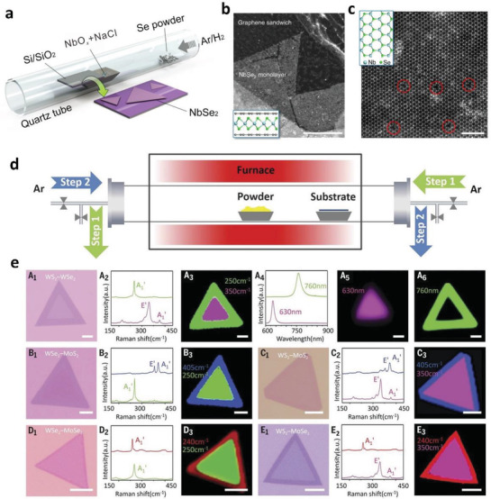
a) A typical CVD setup used to fabricate NbSe2 nanosheets. b) A low‐magnification annular dark‐field STEM (ADF‐STEM) image of single‐layer NbSe2 NSs encapsulated by the graphene sandwich. c) Atomic resolution ADF‐STEM of NbSe2 demonstrating the hexagonal crystal structure. a–c) Reproduced under the terms of the CC‐BY Creative Commons Attribution 4.0 International License (http://creativecommons.org/licenses/by/4.0/).[ 106 ] Copyright 2017, The Authors, published by Springer Nature. d) Modified CVD system with reversible Ar flow for the epitaxial growth of the lateral TMDs heterostructures. e) Optical microscopy images for the grown various 2D NSs with lateral heterostructures using the setup and their corresponding characterizations. d,e) Reproduced with permission.[ 119 ] Copyright 2017, The Authors, published by American Association for the Advancement of Science.