
Figure 2.
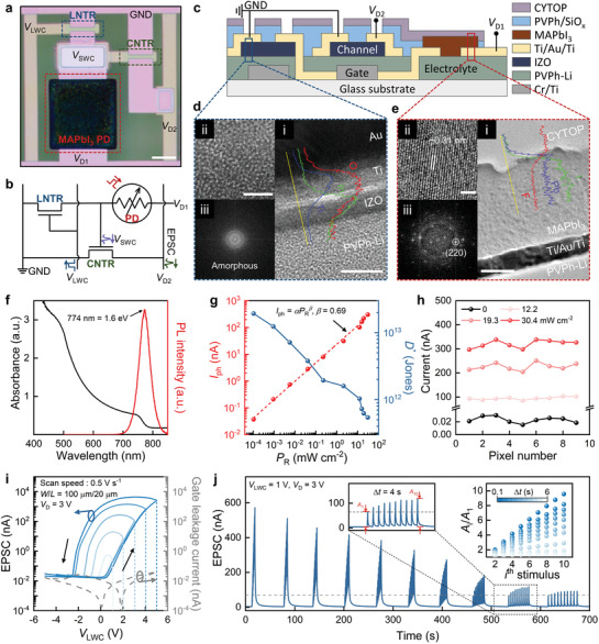
Structural and electrical characteristics of MAPbI3 PD and LNTR. a) Optical microscopy image of a DAVAN device, consisting of one MAPbI3 PD and two Li‐NTR (LNTR and CNTR). The MAPbI3 film is patterned on a designed circuit (scale bar: 100 µm). b) Circuit and c) schematic cross‐sectional structure of a DAVAN device. d) Cross‐sectional HR‐TEM image and corresponding EDS line scan profiles of O (red), Ti (blue), and In (green) obtained from the IZO channel of Li‐NTR (scale bar: 10 nm) (i), enlarged IZO area (scale bar: 2 nm) (ii), and an FFT image of the amorphous IZO channel (iii). e) Cross‐sectional HR‐TEM image and the EDS line scan profiles of F (red), Pb (blue), and I (green) from the MAPbI3 PD (scale bar: 100 nm) (i), enlarged MAPbI3 area (scale bar: 2 nm) (ii), and the FFT image of the crystalline MAPbI3 active area (iii). The results show that the MAPbI3 active layer is in tetragonal phase even after 1 month of exposure to air. This means that the CYTOP polymer perfectly prevented the penetration of moisture from air. f) UV–vis absorption spectra and PL spectra of an as‐synthesized MAPbI3 film on the glass substrate. g) The dependence of the photocurrent and detectivity on different optical power densities. h) The dark current and photocurrent of 9 pixels at different optical power densities. i) Large hysteresis I D–V LWC curves (solid lines) measured in sweep cycles in the range from 1 to 5 V and −1 to −5 V with a scan speed of 0.5 V s−1. The gate leakage current (dashed line) also measured in a sweep cycle of −5 to 5 V. j) The EPSC responses under ten V LWC with different pulse frequencies. The insets show the EPSC response with Δt = 4 s (left) and the current gain (A i/A 1) versus stimulus number (right).