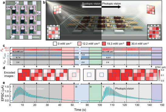
Figure 5.

Characterization of DAVAN device array. a) An optical microscopy image of the 3 × 3 DAVAN device array (scale bar: 500 µm). b) Schematic illustration showing the two sets of optical inputs for image‐encoding and data processing. c) Timing diagram of a pixel of the DAVAN device located in the center of the 3 × 3 DAVAN device array. d) Encoded image sequence in each state of the 3 × 3 DAVAN device array. e) Transient EPSC response of the DAVAN device located in the center of the 3 × 3 DAVAN device array (i–v).
