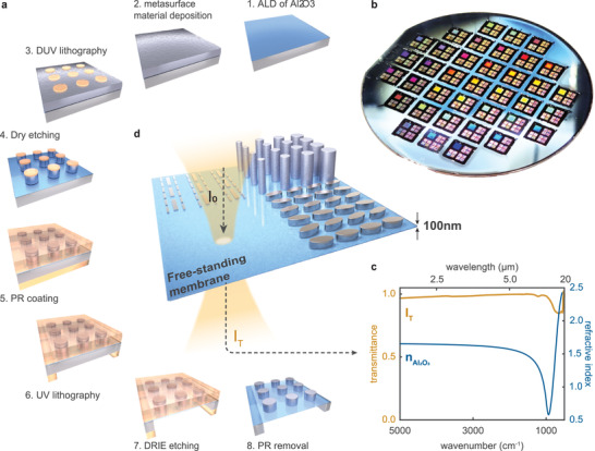
Figure 1.

Wafer‐scale fabrication of membrane‐based metasurfaces. a) Fabrication steps of the membrane‐based metasurfaces. 1) Atomic layer deposition of a 100 nm thick amorphous Al2O3 film. 2) Deposition of metasurface material. 3) DUV lithography for high‐throughput pattern generation. 4) Dry plasma etching. 5) Photoresist coating. 6) UV laser writing for defining membrane openings. 7) Deep reactive ion etching through the wafer. 8) Oxygen plasma for resist removal. b) Photograph of a fully processed 4 in. silicon wafer consisting of large‐area metasurfaces. c) Low refractive index (refractive index data are replotted from data presented in ref. [ 22 ]) and high transmittance throughout an ultrawide spectrum ranging from 2 to 20 µm make the Al2O3 membrane an attractive substrate material for mid‐IR metasurfaces and nanophotonics. d) Illustration of various types of metasurfaces that are fabricated with the reported method, including tilted Ge ellipses supporting high‐Q resonances, Ge nanopillars enabling wavefront and polarization control, and Al‐based multiresonant plasmonic nanorod antennas for label‐free biosensing.
