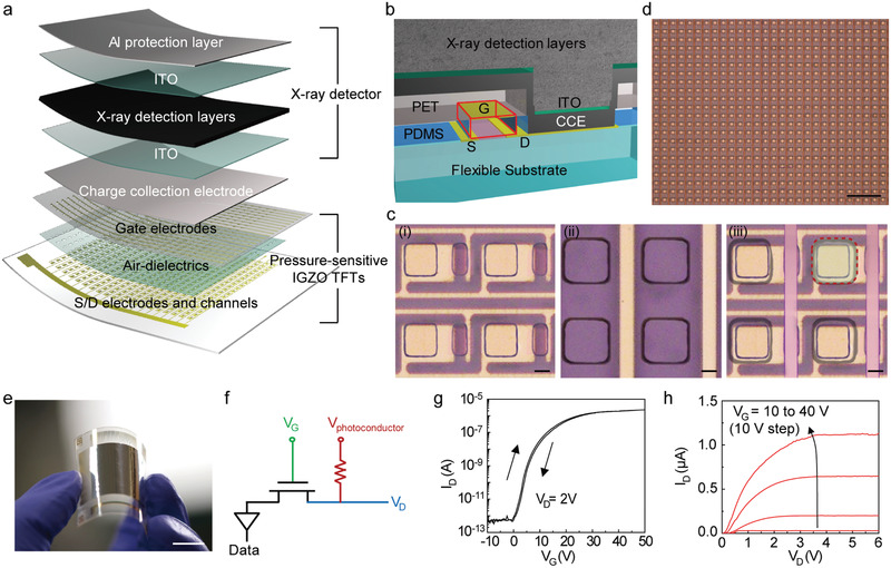
Figure 2.

Integration of the pressure‐sensitive IGZO TFT arrays with the perovskite layer. a) Schematic layouts of the multiplexed detector that consisted of pressure‐sensitive IGZO TFTs and X‐ray detectors. b) Schematic image of the cross‐sectional perspective view of the fully‐integrated multiplexed detector. c) Optical microscopy images before the integration of the perovskite layers. The bottom panel consists of the IGZO channels, S/D electrodes, and elastomeric partition spacers with via holes (i). The top panel consists of the gate electrode and via holes (ii). The bottom and top panel are integrated with the alignment of via holes (iii). Scale bars: 10 µm. d) Optical microscopy image of a high‐resolution pressure‐sensitive IGZO TFT arrays with a pixel pitch of 50 µm. Scale bar: 200 µm. e) Photograph of a flexible, high‐resolution multiplexed detector with a sensing area of 2 × 2 cm. Scale bar: 1 cm. f) Circuit diagram of the multiplexed detector. g,h) Transfer characteristic (V D = 2 V) and output characteristic (V G = 10 to 40 V) of the multiplexed detector.
