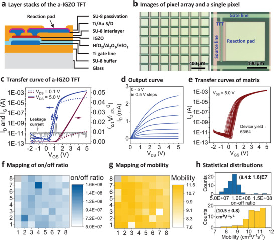
Figure 2.

Structure and electrical performance of the a‐IGZO TFT active‐matrix. a) Schematic layer stacks of the a‐IGZO TFTs. b) Optical microscopy images of the pixel array and a single pixel on the active‐matrix. One pixel consists of a control TFT and a reaction pad. The reaction pad is connected to the drain of the TFT. c) Typical transfer characteristics with V GS from −2 to 5 V for the a‐IGZO TFTs (L = 6.5 µm, W = 200 µm). The leakage current is plotted with gray lines. d) Corresponding output characteristics at V GS from 0 to 5 V in 0.5 V steps. e) Transfer characteristics of all the 63 working TFTs in the 8 × 8 matrix. f,g) Spatial distributions of on/off ratios and mobilities of the a‐IGZO TFT active‐matrix. The dysfunctional pixel is marked with a gray block. h) Histograms of the on/off ratios and mobilities of the 63 working TFTs showing their statistical distributions. The average on/off ratio is (8.4 ± 1.6) × 107, and the average mobility is (10.5 ± 0.8) cm2 V−1 s−1.
