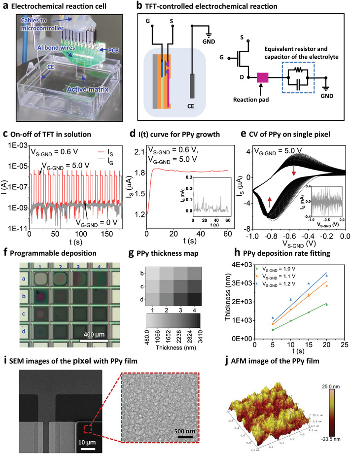
Figure 3.

Digital electrochemistry of PPy on the a‐IGZO TFT active‐matrix. a) Photograph of a two‐electrode electrochemical reaction cell. b) Schematic and circuit diagrams for the TFT‐controlled electrochemical reaction. c) I(t) curve for the on‐off operation of the a‐IGZO TFT in the PPy monomer solution. The V S‐GND is kept as 0.6 V versus Ag/AgCl and the control TFT is turned on and off by switching the V G‐GND between 5 and 0 V. d) Typical I(t) curve for the PPy deposition on a single pixel. V G‐GND = 5 V and V S‐GND = 0.6 V versus Ag/AgCl. The inset shows the leakage current I G plotted versus deposition time. e) CV of the deposited PPy on a single pixel. The V G‐GND is kept as 5 V. The inset shows the leakage current I G during the voltage scan. f) Optical microscopy image showing a 4 × 4 array with PPy programmatically deposited. From row a to row d, the V S‐GND is 0.9, 1.0, 1.1, and 1.2 V versus Au, respectively, and from column 1 to 4 the deposition time is 5, 10, 15, and 20 s, respectively. For all the depositions the V G‐GND is fixed as 5 V. g) Thickness mapping of the deposited PPy corresponding to (f). h) Plot and linear fitting of the PPy thickness versus deposition time at different V S‐GND. i,j) Typical SEM images (SE contrast) and AFM image of the as‐deposited PPy film on the pixel.
