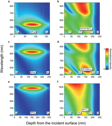
Figure 2.

Optical field distributions of TC‐OPDs. Optical field distributions for exemplary spacer layer thicknesses of a) 107, c) 195, and e) 245 nm are shown. The TC layers have strong resonance, thus lead to high photon absorption in the related active blend of the corresponding OPD (b,d,f) at a similar wavelength. Different layer positions are marked by white dashed lines. The cathode Al thickness is 100 nm for all TC‐OPDs.
