Figure 5.

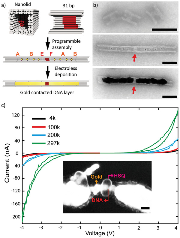
Contacting and conductance of a 10 nm DNA nanolayer. a) Top: design scheme of a nanolid element consisting of a standard mold element containing a central 31 bp (≈10 nm) DNA nanolayer (shown in red) in which the DNA helices align with the mold axis. Middle: Integrating the nanolid element with three AuNP‐loaded mold elements on either side. The letters indicate the employed interfaces. Bottom: Electric contacting of the DNA nanolayer by the growth of Au nanoelectrodes inside the mold elements b) tSEM images of nanolid elements before (top) and after integration (middle) with AuNP‐loaded mold elements and Au nanoelectrode growth (bottom). The red arrows point to the DNA nanolayer. c) Current–voltage characteristics of the DNA nanolayer measured at different temperatures (4, 100, 200, and 297 K). Inset: SEM image of the contacted DNA nanolayer–nanoelectrode assembly. The arrows mark the DNA nanolayer (red), the protective HSQ resist layer (magenta), and the gold nanoelectrodes (orange). The scale bars are 50 nm.
