
Figure 2.
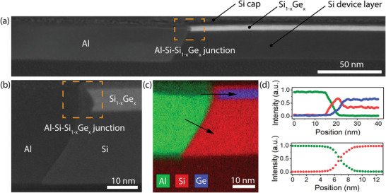
a) Overview HRSTEM image of the entire Al‐Si1−x Ge x ‐Al heterostructure and b) close‐up view of the metal–semiconductor interface. c) EDX map of the Al‐Si‐Si1−x Ge x junction and d) respective EDX linescan across the abrupt Al‐Si‐Si1−x Ge x and Al‐Si interface. The color coding is carried over from Figure 2c.