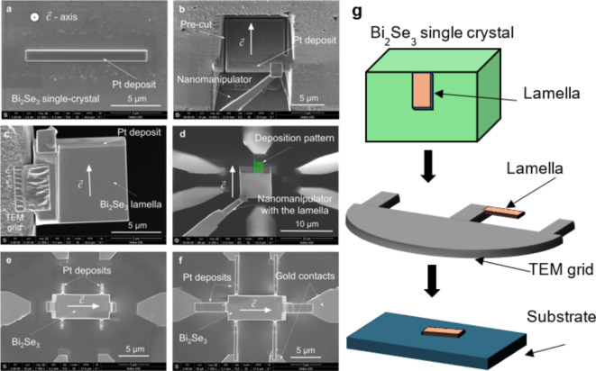
Fig. 1.
SEM micrographs of the fabrication process of the single-crystal device: (a) Protective Pt deposit grown by FIBID. (b) Pre-cut lamella attached to the Omniprobe. (c) TEM grid with the lamella after the cleaning process. (d) Landing of the lamella in the region between the gold pads of the chips. Green rectangle represents the pattern of the Pt deposit by FIBID. (e) First part of the Pt leads grown by FIBID at  . (f) Final functional Bi2Se3 single-crystal device. (g) 3D scheme of the fabrication process, from the starting point in which we have a Bi2Se3 single crystal (fig. a) to the lamella landed on the final substrate (fig. e).

