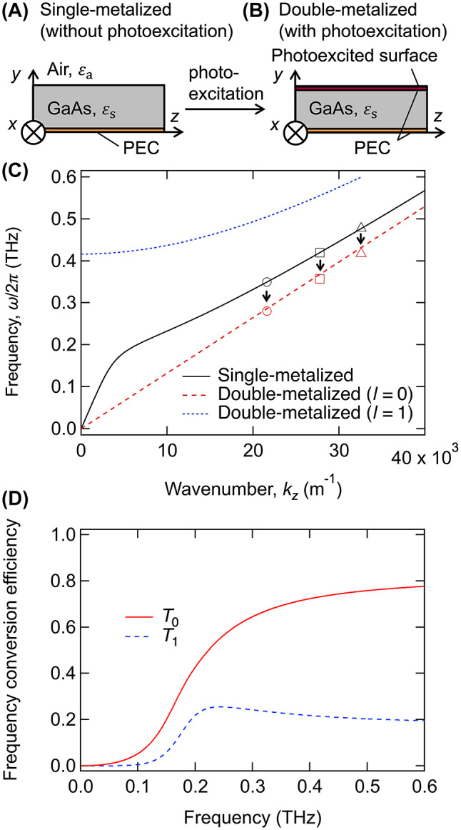
Figure 1:

Schematics of the (A) single-metalized (without photoexcitation) and (B) double-metalized (with photoexcitation) waveguides. (C) Dispersion curves of transverse magnetic (TM) and transverse electromagnetic (TEM) modes in the single- and double-metalized waveguides. In this analysis, the thickness of the waveguide is d = 100 μm, and the relative permittivity of GaAs is ɛ s = 12.96. The input and output frequencies observed in the experiment are plotted using red and black markers, respectively; the circles, squares, and triangles correspond to the frequency conversion for input frequencies of 0.35, 0.42, and 0.48 THz, respectively. (D) Energy efficiency of the frequency conversion T l from the lowest TM mode in the single-metalized waveguide to the TEM (l = 0) and TM (l = 1) modes in the double-metalized waveguide.
