Figure 1:
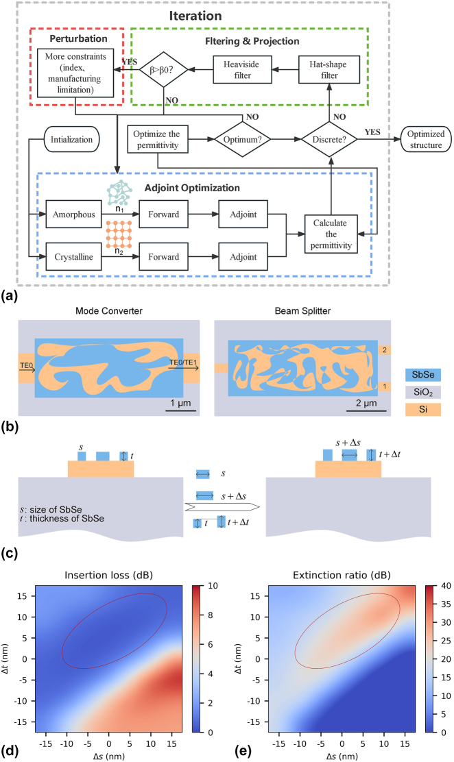
The algorithm architecture of robust inverse design and the robustness analysis of an inversed-designed photonic device. (a) The flow chart of the robust inverse design algorithm. (b) The structural diagram of the MC and OS. (c) The schematic diagram illustrates the dimensional and thickness variations of the Sb2Se3 structure. The IL (d) and ER (e) of the OS, with Sb2Se3 in its amorphous state, were simulated for various sizes (Δs) and thickness (Δt) of the Sb2Se3 pattern. The prominently marked red ellipsoid indicates that OS still exhibits low IL and a high ER at certain fabrication errors.

