Figure 2:
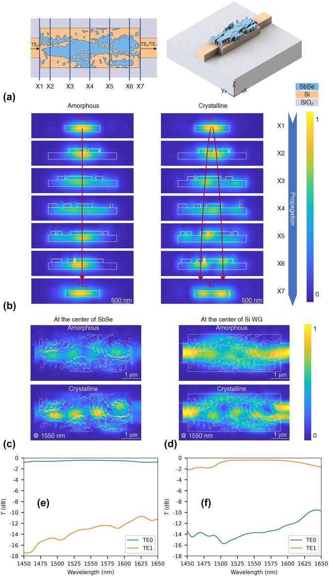
The schematic diagram and performance of the designed MC. (a) The layout and 3D image of the MC. The footprint of MC is 5 μm × 2 μm. X1 to X7 are different positions along the propagation direction of the devices. X1 is positioned in the input waveguide at a distance of 5 nm away from the input port of MC. X7 is located in the output waveguide, 5 nm away from the output port of MC. X2 to X6 is inside MC and has a distance of 0.5, 1.5, 2.5 3.5, 4.5 μm to the input port of MC. (b) The distribution of the electric field (y–z plane) of MC along the propagation direction. (c) The distribution of the electric field (x–y plane) at the center of the Sb2Se3 pattern. (d) The electric field (x–y plane) of MC at the center of the silicon waveguide. The simulated spectra at the amorphous state (e) and the crystalline state (f).

