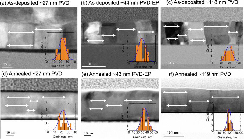
Fig. 1. The microstructure of as-deposited and annealed Cu films.
STEM image of (a–c,) as-deposited ≈27 nm PVD, ≈44 nm PVD-EP, and ≈118 PVD films, respectively. The morphology of these films after annealing at 500 °C is shown in (d–f). The micrographs show the representative area of the as-deposited and annealed films. The grain size distribution of both as-deposited and annealed films is shown in the inset. The grains of these films are columnar. There is no noticeable porosity in the films. Annealing at 500 °C leads to grain coarsening in most of the characterized films, as shown in (e, f) and Table 1.

