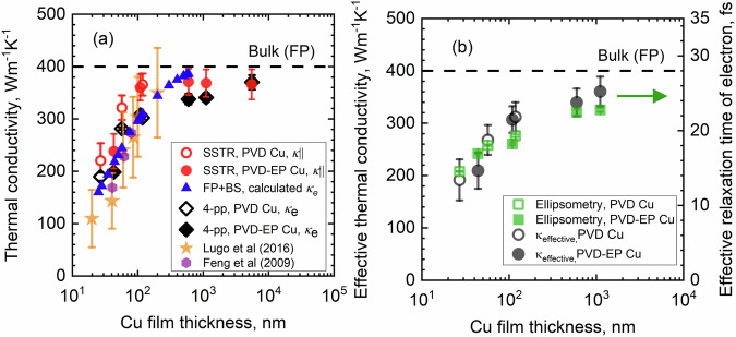
Fig. 3. Thermal transport in Cu film based on its thickness and electron scattering rates.
a In-plane thermal conductivity (k||) of the as-deposited Cu films measured with SSTR is indicated by a red circle symbol. The dashed line represents the calculated bulk thermal conductivity of Cu from our first-principles (FP) calculations. The solid triangle symbol shows the electrical thermal conductivity of Cu film for different thicknesses procured by calculating the total scattering rate of electrons using Matthiessen’s rule to include boundary scattering (BS) of electrons along with the electron-phonon scattering rate obtained from first-principles calculations (FP + BS). SSTR measured in-plane thermal conductivity of the as-deposited Cu films mostly comply with the thermal conductivity of the same films derived from the application of the Wiedemann–Franz law to electrical resistivity measurement (presented by black diamond symbol) assuming the low-temperature value for the Lorenz number. The calculated thermal conductivity using first principles is greater than the experimental value found with the 4-point probe method. This discrepancy happens because our calculations are performed with a constant electron-boundary scattering length of ≈39 nm. However, the grain size of the Cu films (Table 1 and Fig. 1) can be less than ≈39 nm. With a reduced grain size, there is more grain boundary scattering which decreases the measured electrical thermal conductivity38–40 compared to the calculated value. However, our measured thermal conductivities are found to be close to those reported in the previous works for similar film thicknesses34,35. b The effective thermal conductivity (black circle symbol) calculated from the cross-plane and in-plane thermal conductivities shows a thickness-dependent trend similar to the relaxation time of electrons (green square symbol) in different thicknesses of Cu films determined from IR-VASE measurements.

