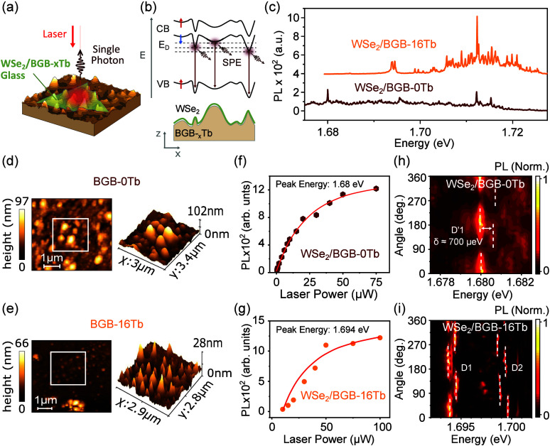
Figure 1.
(a) Schematic representation of the sample with a WSe2 monolayer on polished glass, under laser excitation and showing the emission of single photons. (b) Schematic diagram of the conduction (CB) and valence (VB) band edges of K/K′ valleys. Under local strain, the band edges are deformed and confine excitons that can hybridize with defect levels (ED). The interaction of the confined dark excitons with the defect states generates a single-photon emission. (c) Typical PL spectra of WSe2 monolayers on BGB-16Tb and BGB-0Tb at temperature T = 3.6 K. Several sharp PL peaks are observed for both samples. (d, e) AFM topography image of the glass substrates (0% and 16% Tb3+). The Tb3+ doping affects the topology of the glass after polishing. (f, g) Typical laser power dependencies of PL intensity for the peak at 1.68 eV of the BGB-0Tb glass sample and 1.694 eV of the sample on BGB-16Tb glass, showing a saturation behavior. The solid red lines are a guide for the eyes. All sharp emission peaks show similar saturation behavior. (h, i) Color-coded map of the linearly polarized emission intensity as a function of the angle of in-plane polarization. The same fluctuation was observed for the emissions of each doublet, suggesting that they originate from the same QD. These doublets are separated by δ ≈ 700 μeV.

