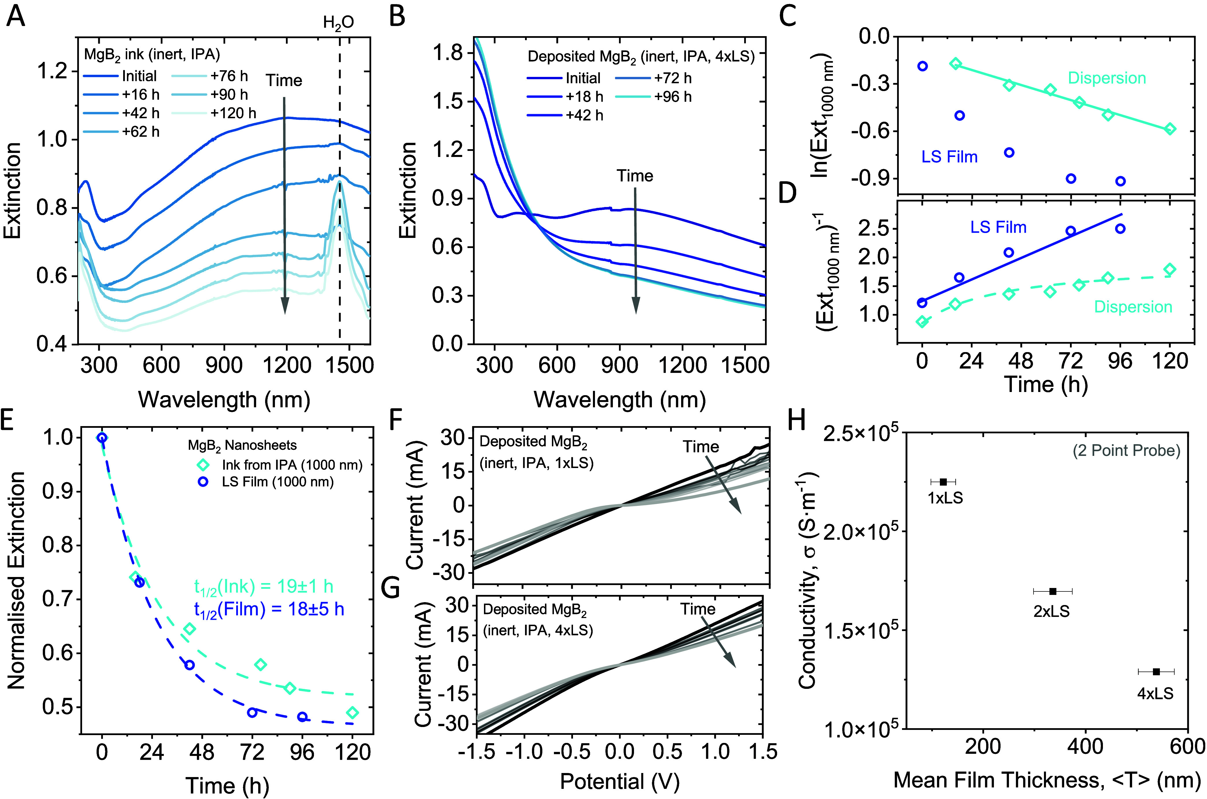
Figure 5.

Nanomaterial stability. (A, B) Change in the extinction of liquid exfoliated MgB2 nanoplatelets in dispersion (A) and after thin film deposition on optical glass (B) as a function of time exposed to ambient conditions. In both cases, a systematic decrease in the overall response is observed for all wavelengths above 450 nm, while the signal below 450 nm undergoes changes in the spectral profile and shows an increased optical density in the UV region, which is indicative of oxide formation. Further, a peak that can be attributed to water forms over time in the nanosheet ink. (C, D) Kinetic plots for rate law analysis of the extinction measurements shown in panels (A, B). Panel (C) shows the change in the natural logarithm of the optical density at 1000 nm, and panel (D) shows the inverse optical density at 1000 nm as a function of time. While the lines indicate a reasonable agreement with a first-order rate law for the dispersed nanomaterial (C) and a second-order rate law for the deposited material (D), the analysis is not unambiguous and is discussed in further detail in the SI. (E) Change in the extinction of the nanosheet ink and thin film at 1000 nm as a function of time. The data can be described by an empirical exponential fit, which allows determination of the material’s half-life. The data for both individual data sets agrees well, and fitting suggests a nanomaterial half-life of 19 ± 1 h and 18 ± 5 h for the nanosheet ink and thin film, respectively. (F, G) I–V characteristics as a function of time for two sets of samples measured after deposition of a single layer (F) and after deposition of 4 layers (G). In both cases, similar systematic changes are observed: the initial ohmic response changes to a more rectifying transport behavior, which is consistent with the formation of an oxide layer. (H) Conductivity of the same MgB2 films measured as a function of the mean film thickness determined by profilometry at different points across the substrate. A decrease in the conductivity is observed with increasing film thickness, which is counterintuitive, and may be attributed to surface oxidation of the nanomaterial during the processing steps.
