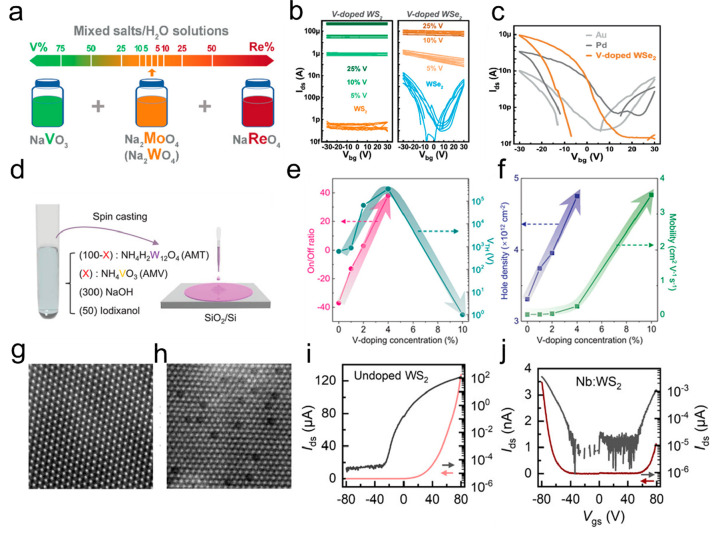
Figure 11.
Synthesis of transition meatal doped TMDs. (a) Schematic illustration of preparing different ratios of mixed salt solutions for the fabrication of Re- and V-doped 2D TMDs. (b) Typical transfer curves of V-doped WS2 and WSe2 monolayers. (c) Transfer characteristics of WSe2–FETs with three kinds of contacts including Au, Pd, and V-doped WSe2. Reproduced from ref (68). Copyright 2021 John Wiley and Sons. (d) Schematic for preparation of V-doped WSe2. (e,f) On/off ratio and threshold voltage (e), as well as the field-effect hole mobility and intrinsic hole carrier concentration (f), vary as a function of V-doping concentration. Reproduced from ref (82). Copyright 2020 John Wiley and Sons. (g,h) HAADF-STEM images of undoped (g) and doped (h) monolayer WS2 crystals. Scale bars are 2 nm. (i,j) Transfer characteristics of undoped (i) and doped (j) monolayer WS2 crystals. Reproduced from ref (65). Copyright 2019 American Chemical Society.

