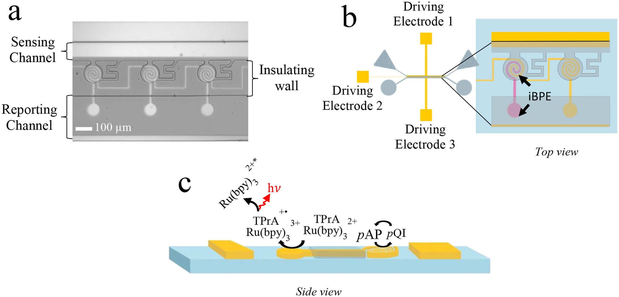
Scheme 1.

(a) Brightfield image of the 5 μm-gap device. (b) Illustration of 5 μm-gap device that zooms into a close-up of driving electrode 2 and BPEs. (c) Side view of the device displaying the reactions occurring at each BPE pole under an applied voltage bias.
