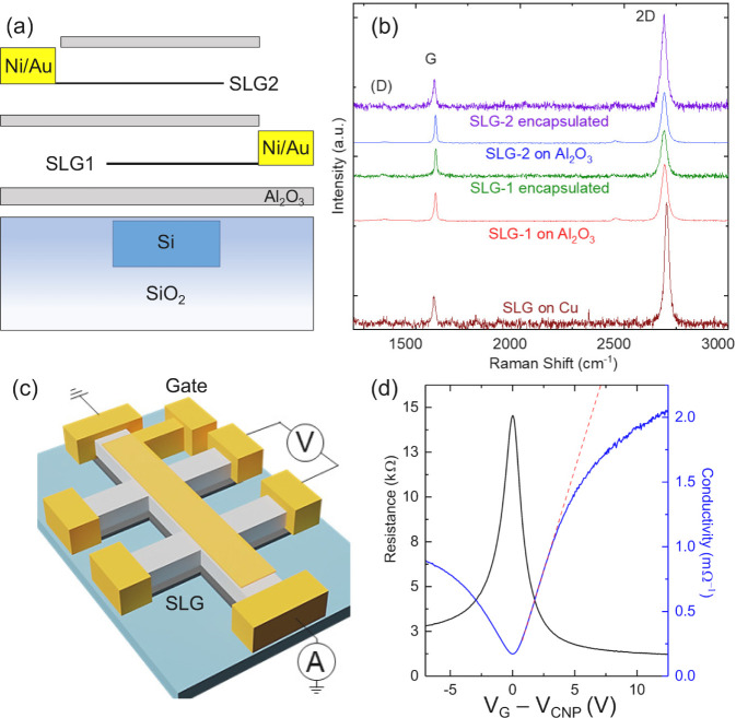
Figure 2.
(a) DSLG modulator fabrication schematic: 10 nm Al2O3 deposition on Si WG with 20 nm Al2O3 between bottom and top SLG. 10 nm Al2O3 is used to encapsulate both SLGs to protect them during subsequent processing steps, minimize contamination, and preserve μ. The bottom encapsulation is used to maintain symmetry between the two SLGs, so that both are in the same environment. (b) Raman spectra at 514 nm for the SLG closest to the WG (SLG1) and that farthest from the WG (SLG2), as-grown on Cu, after transfer, after device fabrication. The spectra are normalized to I(G), with Cu background PL removal.97 (c) Schematic of SLG (gray) on SiO2 (green) top-gated Hall bar with Ni/Au (yellow) contacts. (d) Measured RS (black) and calculated σd.c. (σd.c. = 1RS) (blue). Red dashed line is the σd.c. linear fit for V > 0, showing the transition from linear to sublinear regime for V > 5 V.

