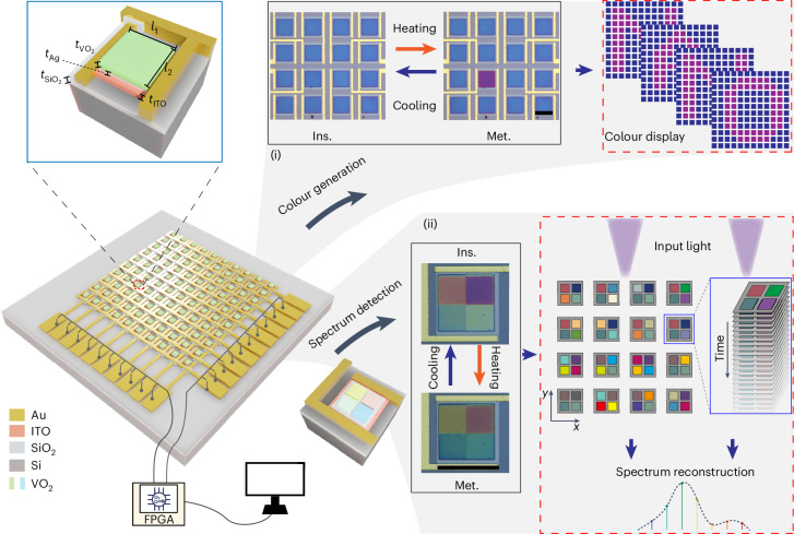
Fig. 1. The schematic diagram for the nanophotonic pixel matrix, controlled with an FPGA and computer.
Each matrix pixel has a cavity consisting of a metal reflective layer and a VO2 layer laid on top of the microheaters made of ITO. The top-left inset shows an enlarged view of a single VO2 pixel, with side lengths of l1 and l2, VO2 thickness of , ITO thickness of tITO, Ag thickness of tAg and SiO2 thickness of . For colour generation of the nanophotonic matrix (i), the electrically programmable matrix is controlled through the row–column scheme, and the entire device works in the refresh mode for display. For spectrum detection of the nanophotonic matrix (ii), each unit spectral pixel consists of 2 × 2 VO2 cavities integrated onto a single heater, which is controlled individually. Every pixel can be regulated to any intermediate state at any time. The black solid boxes in the figure show the optical microscope images of the pixels, and the red dashed boxes show illustrations for display and spectrum detection. Ins., the insulating state; Met., the metallic state. Scale bars, 100 µm in (i) and (ii).

