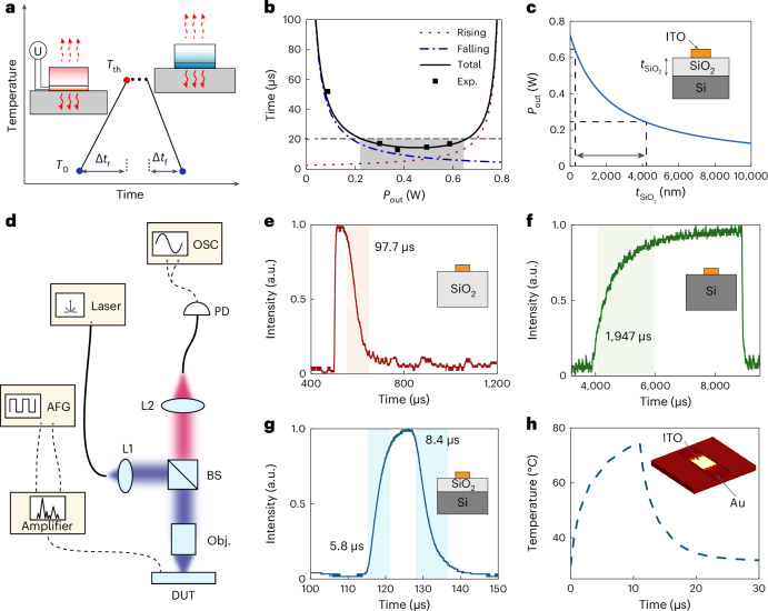
Fig. 3. The optimization for the electrothermal response speed of the VO2 cavities.
a, Illustration of the heating and cooling processes. Here T0 and Tth are the initial and threshold temperatures, Δtr denotes the rising (heating) time and Δtf denotes the falling (cooling) time. The total time is the sum of the rising and falling times. Here the symbol U represents the voltage source. b, The theoretical estimation of rising and falling times for the device as a function of the thermal dissipation power, Pout. The shaded area indicates the Pout needed for a fast response time below 20 µs, and the square dots are the total time of the experimental results. c, The effective output power estimated from the effective thermal conductivity. The arrow indicates the SiO2 thickness region required to obtain a thermal dissipation power Pout within the shaded region in b. The inset shows the cross section of an ITO heater on a SiO2/Si substrate. d, The measurement set-up for the dynamic response. L1(2), lens 1(2); BS, beam splitter; Obj., objective; DUT, device under test; PD, photodetector; OSC, oscilloscope; AFG, arbitrary function generator. e–g, The measured rising and falling times for devices fabricated on different substrates, namely, SiO2 (e), Si (f) and SiO2/Si (g). The shaded area is labelled with the time to reach 90% of maximum or minimum intensity. The insets show the cross sections of the heaters on different substrate configurations. h, The simulated rising and falling times for the device on a SiO2/Si substrate. The inset shows the simulation model. The bright yellow area indicates the hot spot of the temperature.

