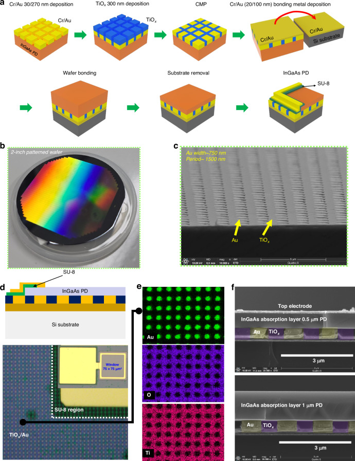
Fig. 2. InGaAs SWIR pixel fabrication integrating with a GMR structure.
a Schematics of the GMR integrated InGaAs PDs by utilizing wafer bonding based thin film transfer method b Photograph of wafer-level patterned GMR structure with 1.5 μm period. c SEM image for periodic patterns consisting of Au width of 0.75 μm and TiOx 0.75 μm. d Schematic image of the fabricated PD on GMR structure and optical image of fabricated devices. e EDX images of Ti, O, and Au atoms at the top view. f Fabricated 0.5 μm and 1.0 μm AL InGaAs PD on GMR Si structure

