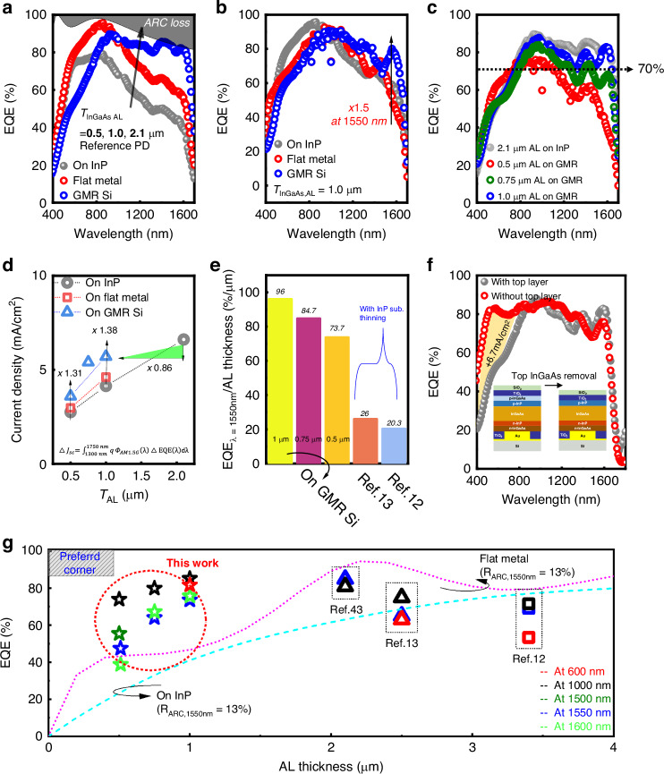
Fig. 4. Spectral absorption characteristics of InGaAs PDs.
a EQE spectra for fabricated PDs on InP substrate with different TAL. b EQE spectra for fabricated 1 μm AL PDs on different bottom structures. c Resulting EQE spectra for different TAL on GMR structure and reference 2.1 μm AL PDs on InP substrate. d Calculated current density using EQE spectrum as a function of TAL and structures. e Comparison of normalized performances of EQE per TAL for proposed devices and conventional PDs. f Fabricated devices with/without 20 nm surface InGaAs layer for 1 μm AL PDs on GMR Si. g Benchmark for state-of-the-art InGaAs-based SWIR pixels with simulated EQE lines as a function of TAL variation (Dashed line: InGaAs PD on InP substrate, dotted line: InGaAs PD on flat metal structure, with the same ARC of this experiment)

