Abstract
This study successfully synthesized high-performance photodetectors based on Ag-WO3 core–shell heterostructures using a simple and economical two-step pulsed laser ablation in water method and has investigated the electrical characteristics of the Ag@WO3 nanocomposite heterojunction. The Hall effect tests indicate that the synthesized Ag@WO3 exhibits n-type conduction with a Hall mobility of 1.25 × 103 cm2V-1S-1. Dark current–voltage properties indicated that the created heterojunctions displayed rectification capabilities, with the highest rectification factor of around 1.71 seen at a 5 V bias. A photodetector’s responsivity reveals the existence of two response peaks, which are situated in the ultraviolet and visible region. The photodetector demonstrates a rapid response time of less than 100 ms. The detectivity values for wavelengths of 350 nm and 490 nm were 35 × 1013 Jones and 28 × 1013 Jones, respectively. The n-Ag-WO3/n-Si photodetector achieved a maximum EQE of 11.5% in the ultraviolet wavelength when subjected to 3 V and illuminated with 350 nm (26 mW/cm2) light. The devices demonstrate rapid switching behavior with a rise time of 0.32 s and a fall time of 0.33 s. The time-dependent light response of a photodetector under illumination at 26 mW/cm2 is seen at a bias of 3 V. The light exhibits a rise and decay duration of 15 s, while the photocurrent gain is measured at 9µA. The photocurrent of devices exhibited a positive correlation with the incoming light intensity, suggesting that the junction has the potential to function as a photo detector.
Keywords: Ag@WO3, Core–shell, Nanocomposite, Photo detection, Pulsed laser ablation
Subject terms: Materials science, Optics and photonics
Introduction
In recent years, the field of nanotechnology has transformed several industries by enabling the development of advanced materials with enhanced properties1,2. Among the various types of nanomaterials, reactive core–shell nanoparticles have emerged as a promising category with numerous applications3,4. These nanoparticles possess a unique structure where a reactive core is encapsulated within a shell, allowing for precise control over their characteristics and functionality5–7. Metal@oxide core–shell nanocomposite materials can be intentionally produced using various well-known methods8,9 or may form naturally under specific conditions. For instance, the exposure of several metal nanoparticles to the environment of an oxygen-wealthy can result in the creation of shells of oxide wrapping them10–12. Intentional oxidation of alloy nanoparticles can result in the formation of a metal oxide shell on a core composed of another metal13–15. Furthermore, oxides may encapsulate metal nanoparticles under catalytic conditions due to strong metal-support interactions. Sometimes, the migration of oxides onto metal particles can be quite subtle, especially if it results in the formation of extremely thin or discontinuous films16–19.
Tungsten oxide, as a readily fabricated and low-cost electrocatalytic material, is considered a promising electrocatalyst. The creation of tungstic acid enhances its electrical conductivity, while the development of oxygen vacancies in WO3 modifies its electrical properties and aids in the degradation of hazardous pollutants20,21. Due to its high melting temperature, toughness, photo electrochromic properties, and mechanical characteristics, it is considered a potential candidate for electrical and optical applications22–24. Nanocrystalline WO₃ has a larger surface area and a higher surface-to-volume ratio for chemical and physical interactions, along with quantum confinement effects that influence charge transport, optical properties, and electronic structure25–27. In addition to the aforementioned excellent surface permeability, it is ideal for a wide range of applications, including gas sensors, photo electrocatalysis, efficient water splitting, memory devices, high-temperature diodes, and photodetectors28–34. In recent years, there has been limited information about WO₃ photodetectors utilizing individual nanostructures, as they exhibit slow response times and a low current on/off ratio35–37.
An ideal photodetector should exhibit minimal dark current to reduce interference noise and maximize sensitivity, enhancing the detection of optical signals. It is important to note that the performance of photodetectors generally hinges on the band gap characteristics of metal oxides and semiconductors. WO₃, for instance, is a typical wide band gap semiconductor with a range of 2.6–3.0 eV, a high exciton binding energy of about 0.15 eV, and an optical absorption coefficient ≥ 10,000 cm⁻138–41. This restricts its optical responsiveness in the visible range of the electromagnetic spectrum for photocatalytic applications. Therefore, altering the band gap of WO₃ is crucial as it determines the energy required for generating electron–hole pairs42–44. The band gap of WO₃ resonates with incident ultraviolet light energy, enabling the generation of additional electrons to contribute to photocurrent, thereby enhancing the photodetector characteristics. These physical characteristics indicate that WO₃ semiconductors have significant potential for manufacturing high-performance visible light and UV detectors with reliable performance45,46.
Metal particles like Ag act as localized surface plasmons (LSPs), which involve electromagnetic waves coupled to collective electron oscillations. Incorporation of Ag can modify the band gap of WO₃, extending the spectral response of Ag-WO₃ core–shell heterostructures into the visible range47,48. Nanoparticles of noble metals, such as silver and gold, have attracted significant technical attention due to their unique chemical, catalytic, optical, and electronic properties. The optical characteristics of silver and gold nanoparticles (NPs) are controlled by tunable local surface plasmon resonances. These resonances result from the collective oscillations of free electrons on the nanoparticle surface, which are induced by the incident optical field. All of these can lead to the enhancement of both absorption and scattering processes. The spectrum of the plasmonic relies on the NP size, shape, composition, environment medium, and morphology of the surface49,50.
The modification of nanoparticle surfaces with noble metals has been considered an efficient method to improve the sensing performance of semiconductor gas sensors. This modification has been applied in various heterogeneous photocatalysis applications. Nanostructures of noble metals deposited on a photocatalyst have been found to enhance light response and improve charge transfer efficiency across surfaces, thereby boosting photocatalytic activities and overall efficiency51–55. Furthermore, nanostructures of noble metals have been widely applied across various scientific and technological disciplines, such as agriculture, antimicrobial applications, therapy, diagnosis, and especially in the biomedical and biological fields56–60.
Experimental work
In this study, Ag@WO3 core–shell nanoparticles (NPs) were synthesized using a two-step laser ablation procedure in distilled water. In the first step, a pulsed beam from an Nd laser at 1064 nm was used to cut a 99.9% pure silver plate target, which was 0.8 mm thick. After that, it was immersed in 3 ml of distilled water in a glass container. It should be noted that chemicals were not added to distilled water. In this step, 1 Hz repetition rate, a 10 cm focal length of the lens, and a 15 ns pulse duration were also used. The silver target was cleaned by submerging it in acetone and washing it in clean water prior to dipping and irradiation. The laser ablation procedure was performed on the Ag target employing a 6.12 J/cm2 laser fluence and laser pulse numbers of 200, 250, 300, 350, and 400 pulses. These were done with various concentrations of silver, and the product is the nanoparticle in suspension form (0.36, 0.76, 1.2, 1.6, and 1.96) μg/mL.
In the second step, the silver target was replaced with a tungsten target in the solution to produce the Ag-WO3 colloidal core–shell structure. This step involved using a 1064 nm laser with a focal length of 10 cm, operating at 1 Hz with a constant laser fluence of 76.34 J/cm2 and 300 laser pulses. This condition was the optimum conditions that was achieved previously in our published article, were the optical, structural, morphological, and electrical characteristics of the Ag@WO3 meso porous core–shell have been discussed extensively61. Hall measurements were conducted to assess the electrical conductivity and conductivity type of the Ag@WO3 film. The core–shell Ag@WO3 nanoparticles (NPs) were produced and then deposited onto a single-crystalline n-type silicon substrate via the drop casting process to create an n-Ag@WO₃/n-Si heterojunction (HJ) photodetector. The silicon substrate employed in this study is an n-type material with a mirror-like surface. It has an electrical resistance of 3Ωcm and an orientation of (111), and its thickness is 350 nm.
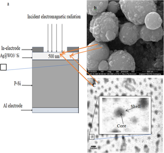
Initially, the silicon substrate was cut into pieces with an area of 1 cm2. Subsequently, it was thoroughly cleaned using a conventional technique and subjected to HF etching for a brief duration to remove the native oxide layer. A 500 nm-thick layer of core–shell Ag@WO3 was then applied. Ohmic contacts were formed by depositing indium and aluminum films onto the Ag@WO3 layer and silicon substrates, respectively, using a thermal resistive method with a specially developed thin metal mask. Figure 1 depicts the cross-sectional view of the n-Ag@WO3/n-Si heterojunction. The current–voltage properties of the heterojunction were investigated under both dark and illuminated conditions at room temperature. The photosensitivity of the photodetector was quantified by measuring its response to light in the spectral range of 300 to 900 nm, using a calibrated monochromator. The rise time of the n-Ag@WO₃/n-Si heterojunction photodetectors was determined using a 200 MHz storage oscilloscope and 100 ns laser pulses emitted by a diode laser operating at a wavelength of 850 nm.
Fig. 1.
Cross-sectional view of heterohunction photodetector a- constructed devce n- Ag@WO3 / Si , b) SEM Image of the active layer Ag@WO3, c) TEM image of the active layer Ag@WO3.
Results and discussion
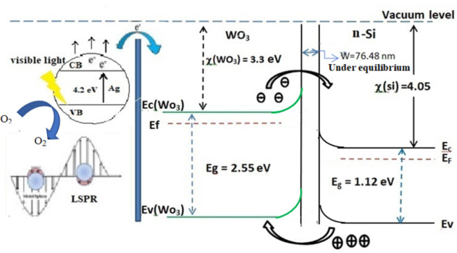
Fabricated high-performance Ag-WO3 core–shell heterostructures photodetectors by using two-step pulsed laser ablation in liquid PLA. This technique was used in this study as it is simple and cost-effective technique61–64. The optical, structural, morphological, and electrical characteristics of the Ag@WO3 mesoporous core–shell material have been presented in a previous study65–68. As shown in Fig. 2, the energy band diagram of the Ag@WO3 nanocomposite is depicted under illumination. When exposed to light with photon energy hvhvhv, WO3 undergoes electron excitation from the valence band to the conduction band. Some of these electrons become trapped at defect levels (DL). Electrons in Ag nanoparticles (NPs) acquire greater kinetic energy due to electron transfer from the defect levels in WO3. The transfer of these electrons from the conduction band of WO3 to the localized surface plasmon level in Ag NPs69–72 is responsible for the photodetector’s increased current. The interfaces of Ag-WO3 nanoparticles heterostructures have an important influence on the separation and charge transfer mechanisms73,74. This is caused by the Ag nanoparticle which acts as a localized surface plasmon. The separation process relates the combination of electromagnetic waves to electron oscillations75,76. Figure 2 also shows that the mechanism decreases the band gap in the core shell structure. The tailored band gap allows for more interaction with visible light in core shell heterostructures (CSNH) compared to controlled WO3. The CSNH shows potential as a photocatalyst due to its capability to adjust the band gap characteristics.
Fig. 2.
Illuminated energy band tuning in n-Ag@WO3/n-Si heterojunction under reverse bias.
To calculate the depletion width W we need to determine the built in potential Vbi77–79.
| 1 |
NA ≫ ND Thus:
To estimate the depletion layer width W the following formula has been used80,81:
| 2 |
where: W = depletion layer, Vbi = built in potential in volts, Nd = n-type donor atom concentrations, Na = p-type acceptor atom, n = concentration of electrons, Kt/q = thermal voltage, T = temperature in Kelvin, q = charge in coulombs. The obtained value found to be about 76.48 nm which represent the depletion region width at equilibrium, where it value has to change under reverse bias82–84.
The Hall Effect measurement results indicate that the produced Ag-WO3 NPs layer exhibits n-type conductivity. Table 1 presents the electrical resistivity and mobility values of Ag-WO3 NPs. The high mobility may be related to the strong localized surface Plasmon resonance (LSPR) exhibited by Ag nanoparticle, which enhances the local electromagnetic fields. This enhancement may improve the charge carrier generation and separation efficiency in the WO₃ shell, leading to increased mobility.
Table 1.
Electrical resistivity and mobility of Ag-WO3 NPs.
| Ag-concentration (µg/ ml) | Mobility (cm2 V-1 s-1)*103 | Electrical resistivity (Ω cm)*104 |
|---|---|---|
| 1.6 | 1.25 | 6.71 |
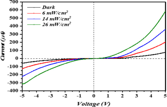
Figure 3 illustrates the current–voltage (I-V) characteristics of the n-Ag-WO₃ NPs/n-Si heterojunction, subjected to a biasing range of (-5 to 5) V. These characteristics were obtained using pulse laser ablation at an Ag concentration of 1.6 µg/ml. Under forward bias, the current shows exponential growth with increasing voltage. Conversely, under reverse bias, the current also increases with voltage; however, no saturation or sharp breakdown was observed due to the dominance of edge leakage current at the contact periphery and additional carrier generation in the depletion region. The illustration demonstrates that the heterojunctions have rectification features. These photodetectors exhibit two distinct regions when a forward current is applied. In the initial area, when a low voltage is applied, a little current is generated by the photodetectors, which is referred to as recombination current. The generation of this current occurs when an electron, which has been stimulated from the valence band to the conduction band, recombines with a hole in the valence band to restore balance85.
Fig. 3.
Current–voltage characteristics of the photodetector under various illumination conditions.
The second region is characterized by the presence of forward current, which is referred to as the diffusion current. In this region, the current exponentially increases when the bias voltage potential exceeds the potential barriers. This bias voltage provides sufficient energy for electrons to overcome the barrier height and move forward. Figure 3 presents and illustrates the current–voltage (I-V) characteristics of the n-Ag-WO₃/n-Si heterojunction at room temperature. Measurements were taken in both forward and reverse directions, with a bias voltage ranging from -5 V to + 5 V. The heterojunction was tested under varying illumination conditions. The rectification ratio depends on the illumination conditions at 4.5 V. The figure can also show that the forward currents in all heterojunctions increase with applied bias voltage. Further, when the light intensity increases, this can result in higher forward currents, which can be attributed to reduced Ag-WO₃ resistance. The turn-on voltage ranges from 3.5 to 4.5 V, depending on illumination. Non-ohmic contacts are indicated by nonlinear I-V curves. The devices exhibited higher photocurrent (I_Photo) values across all illumination conditions compared to dark current (I_Dark) values at all bias voltages. Incorporation of silver (Ag) nanoparticles (NPs) resulted in enhanced device photostability.
The explanation for this discovery lies in the comparative band alignment analysis of WO₃ and Ag. The Fermi level of Ag (E_F = -4.7 eV) is positioned below the conduction band edge of WO₃. Electron transfer from the conduction band (CB) of WO₃ to the Fermi level (E_F) of Ag can occur effectively. All these can show that Ag nanoparticles (NPs) can act as electron reservoirs. This can be attributed to two reasons: (1) it can capture electrons which are generated during photoexcitation, and (2) it can reduce electron–hole recombination (thereby increasing exciton lifetime). Additionally, Ag NPs can efficiently transport electrons to the electrode. The presence of Ag NPs on the surface of WO₃ NPs reduces the accumulation of electrons at oxygen vacancy sites upon repeated exposure to light. This is because the energy level of Ag is near the conduction band (CB), while defect states typically lie deep within the band gap86,87.
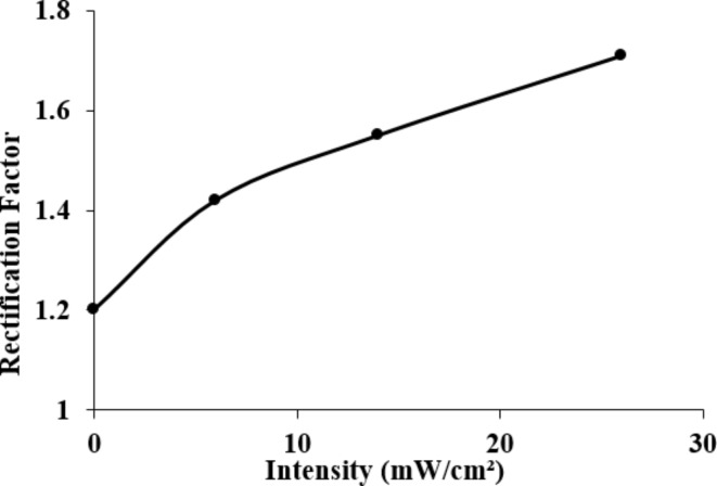
The Ag-WO3/Si heterojunction acheived a rectification ratio of 1.718 at an illumination intensity of 26 mW/cm2, which is the highest observed value. Figure 4 demonstrates that the rectification factor of the n-Ag-WO3/n-Si HJ increases as the illumination level increases.
Fig. 4.
The variations in the rectification factor as a function of illumination for n-Ag-WO3/n-Si photodetector.
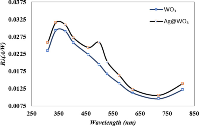
Figure 5 depicts the spectral responsivity curve of n-Ag-WO₃/n-Si heterojunction photodetectors at 26 mW/cm2 and 3 bias voltages. The n-Ag-WO3/n-Si heterojunction exhibits a responsivity located at a wavelength of (350) nm, measuring approximately 0.032 AW-1. Second peak was seen at a wavelength of (490) nm, and the maximal responsivity was measured to be 0.026 A/W. The UV peak observed in the responsivity of Ag/WO₃ core–shell compared with the WO3/Si device could be attributed to many factors related to the unique optical properties of both the silver (Ag) core and the tungsten trioxide (WO₃) shell as a new composite system. Some of these factors are the strong localized surface Plasmon resonance exhibits by the silver nanoparticles (LSPR) in the Uv region. This LSPR occurs when the conduction electrons on the Ag surface of the resonate with incident light at specific wavelengths (the collective oscillation of electrons at the surface), leading to enhanced absorption and scattering of light. In addition, the (LSPR) of the silver core can couple with the excitonic transitions in the WO₃ shell. This plasmon exciton coupling can enhance the optical response in the UV region, this was shown previously in other work87–90.
Fig. 5.
Photo-responsivity of the photodetector that was created, measured at an intensity of 26 mW/cm2 and with a bias of 3 V.
Second peak was seen at a wavelength of (490) nm, and the maximal responsivity was measured to be 0.026 A/W. The UV peak observed in the responsivity of Ag/WO₃ core–shell structures can be attributed to many factors related to the unique optical properties of both the silver (Ag) core and the tungsten trioxide (WO₃) shell as a new composite system. Some of these factors are the strong localized surface Plasmon resonance exhibits by the silver nanoparticles (LSPR) in the Uv region. This LSPR occurs when the conduction electrons on the Ag surface of the resonate with incident light at specific wavelengths (the collective oscillation of electrons at the surface), leading to enhanced absorption and scattering of light. In addition, the (LSPR) of the silver core can couple with the excitonic transitions in the WO₃ shell. This plasmon exciton coupling can enhance the optical response in the UV region; this was shown previously in other works87–90.
The photoexcited electrons are transferred from silver nanoparticles (Ag NPs) to tungsten trioxide (WO3), resulting in an enhancement of the charge-collecting efficiency. This may enhance the heterojunction photosensitivity91–93. Moreover, the inclusion of Ag NPs provides a substantial surface area, resulting in a considerable increase in the absorption coefficient of WO3 (thus enhancing light trapping) and improving the shape of WO3 NPs94,95. Thus, the results demonstrate that core–shell heterostructures with type II band alignment can be effectively constructed at the n-type Ag core-WO₃ shell/n-type Si interface. This process has shown that it enhanced the performance of photodetectors. This can reflect the potential of Ag-WO₃ core–shell nanocomposites as promising materials for the development of highly compact photodetector devices in the future.
To determine the specific detectivity D* of the photodetector, the subsequent equation was applied96–98:
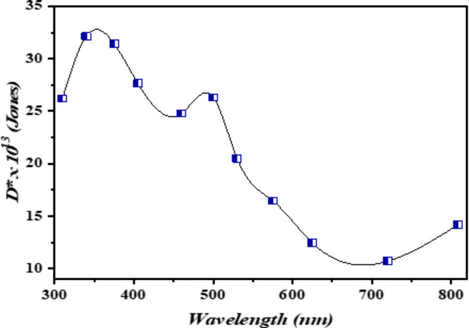
The sensitive area of the photodetector is denoted as ADA_DAD, the bandwidth as Δf\Delta fΔf, and the noise current as InI_nIn. Figure 6 illustrates the specific detectivity of n-Ag-WO₃/n-Si heterojunctions under 26 mW/cm2 and 3 bias conditions. For the n-Ag-WO₃/n-Si device, the detectivity values at wavelengths of 350 nm and 490 nm are 35 × 1013 Jones and 28 × 1013 Jones, respectively. The specific detectivity of the photodetector depends on both responsivity and noise current. Ag-WO₃/Si photodetectors show optimal specific detectivity at UV and visible wavelengths comparable to or better than that of pn silicon photodiodes and broad bandgap heterojunction-based silicon photodetectors99–101.
Fig. 6.
Photodetectivity of the prepared photodetector at 26 mW/cm2 and 3 bias.
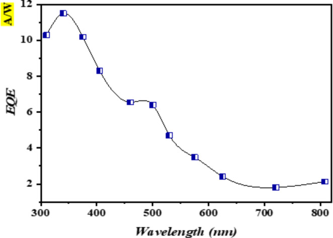
In this study, the external quantum efficiency (EQE) was determined by calculating its dependence on the wavelength of the photodetector. Figure 7 displays the external quantum efficiency (EQE) of the heterojunction (HJ) photodetectors. The synthesized photodetector exhibited a peak external quantum efficiency (EQE) of approximately 11.5% at a wavelength of 350 nm and approximately 6.8% at a wavelength of 490 nm. These results are attributed to the generation of electron–hole pairs for each incoming photon102–105.
Fig. 7.
The external quantum efficiency of the photodetector at 26 mW/cm2 and 3 bias.
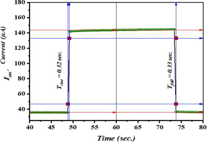
The response-recovery time of photocurrent is a crucial characteristic for investigating the operational mechanism of photodetectors. This measurement not only provides insight into the time required to reach a steady-state condition but also reveals transient-state phenomena, such as carrier trapping during on-and-off cycles. Transient short-circuit photocurrent measurements were used to investigate the ascent and descent transient responses. Figure 8 displays the transient photocurrent responses of n-Ag-WO₃/n-Si devices when exposed to a square pulse of light lasting 1 ms. The rise and fall times of the devices were determined based on the duration required to transition from 10 to 90% of the complete response and from 90 to 10% of the full response, respectively106–108. The n-Ag-WO₃/n-Si devices exhibit rapid on/off dynamics, with a rise time of 0.32 s and a fall time of 0.33 s.
Fig. 8.
Displays the response and recovery time of the fabricated photo detector.
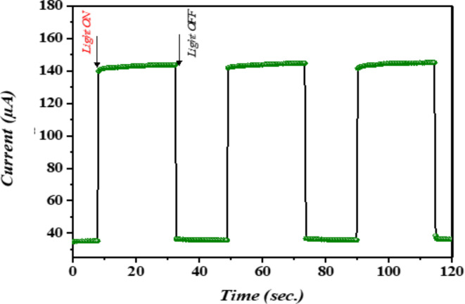
Figure 9 demonstrates the time dependence of the photo response at a 3 V bias of an n-Ag-WO3/n-Si-based photodetector under illumination at 26 mW/cm2. It shows a rise and decay time of 15 s for illumination and a photocurrent gain of 9 µA. The primary requirements for a photodetector to be quick and stable are two. The first one involves the enhancement of the lifetime of the exciton pair. This can be done by fully separating the electron (e-) and hole (h +) components. The second one is the rapid recombination of the electron–hole pair in the absence of external factors. The first element enhances the photocurrent gain, while the second factor reduces the reaction time. Both of these two requirements can result in the improvement of the speed of the device. The Ag-WO3/Si photodetector demonstrates remarkable photo responsive reversibility and stability, consistently generating a stable photocurrent.
Fig. 9.
The time-resolved properties of the photodetector.
The dominant localized surface plasmon resonance (LSPR) band of Ag NPs enhances the absorption efficiency of visible light in the heterostructure. Additionally, the epitaxial interface between the metal and semiconductor facilitates efficient charge transfer from the semiconductor to the metal. Furthermore, the coupling between plasmons in metals and plasmons in semiconductors potentially enhances the absorption efficiency in the near-infrared (NIR) region. The photoexcited electrons are transferred from silver nanoparticles (Ag NPs) to tungsten trioxide (WO3), resulting in an enhancement of the charge-collecting efficiency. This may enhance the heterojunction photosensitivity. Moreover, the inclusion of Ag NPs provides a substantial surface area, resulting in a considerable increase in the absorption coefficient of WO3 (thus enhancing light trapping) and improving the shape of WO3 NPs as shown in other work91–94.
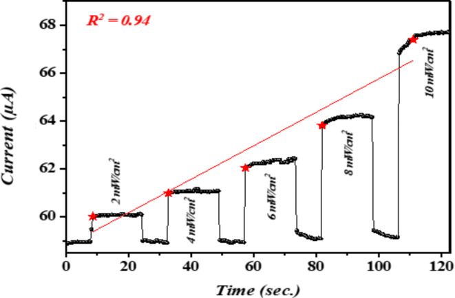
The study also demonstrated that the photocurrent increases when the n-Ag-WO3/n-Si heterojunction is illuminated due to its radial core–shell architecture, which creates a type II band alignment. This alignment reduces the recombination of photogenerated charges and enhances the efficiency of collecting photogenerated charge carriers109–111. Figure 10 illustrates the time-dependent photo response of a photodetector based on an n-Ag-WO3/n-Si heterojunction. The photodetector was biased at 3 V and illuminated at intensities of (2, 4, 6, 8, 10) mW/cm2. The observed enhancements in photocurrent gain, rise, and decay duration can be attributed to the enhanced geometry of the Ag-WO3 core–shell nanocomposite, where the Ag core and WO3 shell are in direct contact. Additionally, an increase in the photocurrent over time was noted under light exposure. This can be related to the effect of heating caused by illumination.
Fig. 10.
Illumination power dependence characteristics of the photodetector.
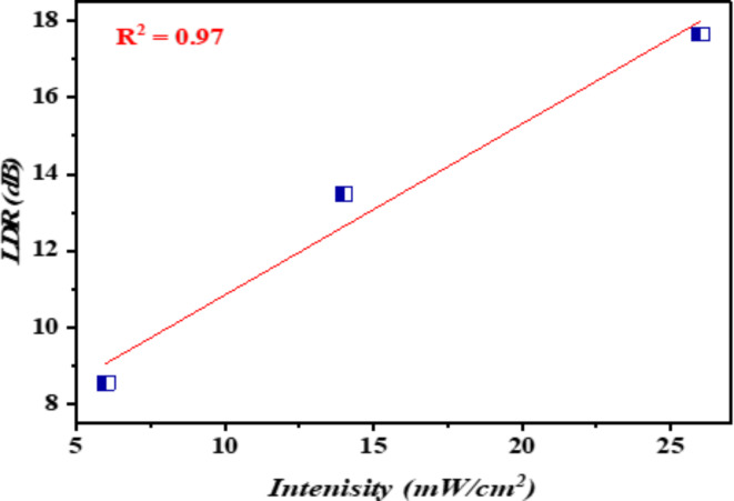
Figure 11 depicts the relationship between the intensity of white light and the photocurrent of the n-Ag-WO3/n-Si device at a bias of 3 V and 26 mW/cm2. The photocurrent of n-Ag-WO3/n-Si devices exhibited a positive correlation with the incoming light intensity. This can suggest that the n-Ag-WO3/n-Si junction has the potential to function as a photo detector. As the samples were exposed to different levels of light intensity, the resistance of all samples decreased. This can be attributed to the generation of more electron hole-pairs. The study also revealed that the incorporation of silver nanoparticles (Ag NPs) enhances the photocurrent of the photodetector by promoting the formation of electron–hole (e–h) pairs. This indicates that the resulting n-Ag-WO3/n-Si photodetectors exhibit strong linearity properties (dynamic range).
Fig. 11.
Linear dynamic range of the photodetector at 26 mW/cm2 and 3 bias.
The performance characteristics of our device are presented in Table 2. They are also compared with various photodetectors (PDs) reported in previous studies operating within a wide band gap. From the comparison presented in Table 2, it is evident that our core–shell Ag@WO3 NPs-based device demonstrates exceptional performance, characterized by a wide band gap and ultrafast photo response.
Table 2.
Illustrates the performance parameters of the Ag@WO3 core–shell NPs/Si-based PD (designed in this study), compared to other reported PDs operating within a wide band gap.
| Photodetector | Bias (V) | Responsivity (mA W-1) | Detectivity (Jones) | Rise/fall time (ms) |
|---|---|---|---|---|
|
Ag@WO3 core–shell (This work) |
3 | 0.032 @ 350 nm | 35 × 1013 at 350 nm | 320 / 330 |
|
Ag@WO3 core–shell (This work) |
3 | 0.026 @ 490 nm | 28 × 1013 at 490 nm | |
| MoS2/GaN NRs/Si112 | 0 | 1.42 × 10⁴ @ 900 nm | 2.72 × 10¹³ | 0.039 / 0.008 |
| MoS2/AlN/Si113 | 0 | 9.93 @ 900 nm | _________ | ____/___ |
| WO3−δ films114 | 2 | 0.12 @ 365 nm | 2.1 × 10¹⁰ | ____/___ |
| n-Bi2Se3/p-GaN115 | 3 | 24,554 | _____________ | 63 / 43 |
| MoTe2/monolayer graphene116 | VD = 1 | 9.71 × 10⁵ @ 1064 nm (202 mW) | 1.55 × 10¹¹ | 78/375 |
Conclusion
This study has made a significant contribution as it presented a device of n-Ag-WO3/n-Si photodetector. Specifically, we produced a sensitive and rapid n-Ag-WO3/n-Si photodetector for detecting light signals using Ag-modified WO3 NPs. The fabricated n-Ag-WO3/n-Si heterojunction photodetectors exhibit excellent UV and visible sensitivity. The current–voltage properties shows that heterojunctions may rectify, with a maximum rectification factor of 1.71 at 5 V bias. Photodetectors have ultraviolet and visible response peaks. These response peaks correspond to Ag@WO3 NPS absorption edges. The detectivity values for 350 and 490 nm were 35 × 1013 Jones and 28 × 1013 Jones, respectively. The n-Ag-WO3/ n-Si photodetector has a maximum UV EQE of 11.5% at 3 V voltage and 350 nm (6 mW/cm2) light. Rapid switching is shown in n-Ag-WO3/n-Si devices. The devices rise and descend in 0.32 and 0.33 s, respectively. At 3 V bias, an n-Ag-WO3/n-Si photodetector shows its time-dependent light response under 26 mW/cm2 illumination. The light rises and decays in 15 s, with a photocurrent increase of 9 µA.
The photocurrent of n-Ag-WO3/n-Si devices correlated positively with the intensity of the incoming light, indicating their potential operation as photodetectors. The results showed that the photodetector performance was enhanced by the formation of core–shell heterostructures with a type II band alignment at the n-type Ag core—WO3 shell—n-type Si interface. The Ag-WO3 core–shell nanocomposite shows significant promise as a material for the future development of highly compact photodetector systems. To fabricate high-speed photodetectors, flexible UV/visible photodetectors, and achieve maximum photocatalytic activity using heterostructures, crucial factors have been identified: metal plasmon-semiconductor exciton coupling, primary absorption of plasmons by metal nanoparticles, and the formation of an epitaxial interface.
Acknowledgements
The authors would like to thank the University of Technology-Iraq for the logistic support this work. The authors extend their appreciation to the Deanship of Scientific Research at Northern Border University, Arar, KSA for funding this research work through the project number “NBU-FFR-2024-1299-03’’. The authors gratefully thank the Prince Faisal bin Khalid bin Sultan Research Chair in Renewable Energy Studies and Applications (PFCRE) at Northern Border University for their support and assistance. The authors would like to thank Warith Al-Anbiyaa University, Karbala, Iraq for the logistic support this work.
Author contributions
Conceptualization, J.A.S., E.T.S., M.H.A., M.A.F., A.S.A., A.B.M.A., S.C.B.G.; methodology, J.A.S., E.T.S., M.H.A., M.A.F., A.S.A., A.B.M.A., S.C.B.G.; validation, J.A.S., E.T.S., M.H.A., M.A.F., A.S.A., A.B.M.A., S.C.B.G.; formal analysis, J.A.S., E.T.S., M. H.A., M.A.F., A.S.A., A.B.M.A., S.C.B.G.; investigation, J.A.S., E.T.S., M.H.A., M.A.F., A.S.A., A.B.M.A., S.C.B.G.; validation, J.A.S., E.T.S., M.H.A., M.A.F., A.S.A., A.B.M.A., S.C.B.G.; resources, J.A.S., E.T.S., M.H.A., M.A.F., A.S.A., A.B.M.A., S.C.B.G.; validation, J.A.S., E.T.S., M.H.A., M.A.F., A.S.A., A.B.M.A., S.C.B.G.; data curation, J.A.S., E.T.S., M.H.A., M.A.F., A.S.A., A.B.M.A., S.C.B.G.; validation, J.A.S., E.T.S., M.H.A., M.A.F., A.S.A., A.B.M.A., S.C.B.G.; writing—original draft preparation, J.A.S., M.H.A,; writing—review and editing, J.A.S., E.T.S., M.A.F., A.S.A., A.B.M.A., S.C.B.G.; visualization, J.A.S., E.T.S., M.H.A., M.A.F., A.S.A., A.B.M.A., S.C.B.G.; validation, J.A.S., E.T.S., M.H.A., M.A.F., A.S.A., A.B.M.A., S.C.B.G.; project administration, J.A.S., E.T.S., M.A.F.; funding acquisition, providing own funds, Each author has reviewed the published version of the manuscript and given their approval.
Funding
The authors extend their appreciation to the Deanship of Scientific Research at Northern Border University, Arar, KSA for funding this research work through the project number “NBU-FFR-2024–1299-03’’.
Data availability
Correspondence and requests for materials should be addressed to Evan T. Salim, Makram A. Fakhri.
Competing interests
This statement serves as an official confirmation that the authors involved in this paper do not possess any conflicts of interest. Furthermore, we assert that the disclosure provided in relation to this publication is comprehensive and accurate, based on the most reliable information available to us. We concur that in the event that we acquire any knowledge suggesting the potential inaccuracy of this declaration or non-compliance with the conflict of interest policy, we will promptly tell the journal.
Footnotes
Publisher’s note
Springer Nature remains neutral with regard to jurisdictional claims in published maps and institutional affiliations.
Contributor Information
Evan T. Salim, Email: evan_tarq@yahoo.com, Email: evan.t.salim@uotechnology.edu.iq
Makram A. Fakhri, Email: makram.a.fakhri@uotechnology.edu.iq, Email: mokaram_76@yahoo.com
Ahmad S. Azzahrani, Email: ahmad.azzahrani@nbu.edu.sa
Ali B. M. Ali, Email: dr.alibasem110@gmail.com
References
- 1.Elhebshi, Y., Alsuwaye, A. & Issa, N.B. A reactive core-shell nanoparticles synthesis, properties and applications in rubber materials. IJARIIE-ISSN (O)-2395-4396. 9(5) (2023).
- 2.Chipara, M., Skomski, R. & Sellmyer, D. J. Electrodeposition and magnetic properties of polypyrrole–Fe nanocomposites. Mater. Lett.61(11–12), 2412–2415. 10.1016/j.matlet.2006.09.024 (2007). [Google Scholar]
- 3.Yahya, A. M., Hassan, A. I., Salim, E. T. & Addie, A. J. Hybrid nanocomposites for enhanced photodetection: Synthesis and application of Ag2O@Graphene/Si heterojunctions. J. Alloy. Compd.1001, 175133 (2024). [Google Scholar]
- 4.De, M., Ghosh, P. S. & Rotello, V. M. Application of nanoparticles in biology. Adv. Mater.20, 4225–4241. 10.1002/adma.200703183 (2008). [Google Scholar]
- 5.Yahya, A. M., Salim, E. T., Hassan, A. I. & Addie, A. J. Ag@Graphene hybrid plasmonic nanocomposites by spray pyrolysis: Synthesis, characterization and improved properties. J. Opt. (India)53(3), 2537–2549 (2024). [Google Scholar]
- 6.Mondal, K. & Sharma, A. Recent advances in the synthesis and application of photocatalytic metal–metal oxide core–shell nanoparticles for environmental remediation and their recycling process. RSC Adv.6(87), 83589–83612. 10.1039/C6RA18102C (2016). [Google Scholar]
- 7.Muhsin, M. S., Salim, E. T. & Saimon, J. A. Structural, morphological and optical properties of tungsten trioxide nanoparticle synthesis by pulsed laser ablation in water: effect of laser fluence. J. Opt. (India)53(3), 2339–2354 (2024). [Google Scholar]
- 8.Colussi, S., Fornasiero, P. & Trovarelli, A. Structure-activity relationship in Pd/CeO2 methane oxidation catalysts. Chin. J. Catal.41(6), 938–950. 10.1016/S1872-2067(19)63510-2 (2020). [Google Scholar]
- 9.Wang, D. et al. The oxidation process and methods for improving reactivity of Al. Crystals12(9), 1187. 10.3390/cryst12091187 (2022). [Google Scholar]
- 10.Fakhri, M. A. et al. Effect of laser fluence on the optoelectronic properties of nanostructured GaN/porous silicon prepared by pulsed laser deposition. Sci. Rep.13(1), 21007. 10.1038/s41598-023-47955-3 (2023). [DOI] [PMC free article] [PubMed] [Google Scholar]
- 11.Zhang, P. et al. Dendritic core-shell nickel-iron-copper metal/metal oxide electrode for efficient electrocatalytic water oxidation. Nat. Commun.9(1), 381. 10.1038/s41467-017-02429-9 (2018). [DOI] [PMC free article] [PubMed] [Google Scholar]
- 12.Wu, C. H., Liu, C., Su, D. & Salmeron, M. B. Bimetallic synergy in cobalt–palladium nanocatalysts for CO oxidation. Nat. Catal.2(1), 78–85. 10.1038/s41929-018-0190-6 (2019). [Google Scholar]
- 13.Yahya, A. M., Salim, E. T., Hassan, A. I. & Addie, A. J. Ag@Graphene hybrid plasmonic nanocomposites by spray pyrolysis: Synthesis, characterization and improved properties. J. Opt. (India). 10.1007/s12596-023-01467-5 (2023). [Google Scholar]
- 14.Luo, Z., Zhao, G., Pan, H. & Sun, W. Strong metal–support interaction in heterogeneous catalysts. Adv. Energy Mater.12(37), 2201395. 10.1002/aenm.202201395 (2022). [Google Scholar]
- 15.Zhang, Q., Lee, I., Joo, J. B., Zaera, F. & Yin, Y. Core–shell nanostructured catalysts. Acc. Chem. Res.46(8), 1816–1824. 10.1021/ar300230s (2013). [DOI] [PubMed] [Google Scholar]
- 16.Muhsin, M. S., Saimon, J. A., Salim, E. T. & Qaeed, M. A. A study beyond laser fluence threshold on WO3 nanoparticle, employing pulsed laser ablation in liquid. J. Opt. (India). 10.1007/s12596-023-01410-8 (2023). [Google Scholar]
- 17.Mirzaei, A., Janghorban, K. & Hashemi, B. Giovanni Neri “Metal-core@metal oxide-shell nanomaterials for gas-sensing applications: a review”. Journal of Nanoparticle Research17(9), 371. 10.1007/s11051-015-3164-5 (2015). [Google Scholar]
- 18.Mendes, P. C. D. et al. Opportunities in the design of metal@oxide core-shell nanoparticles. Adv. Phys.8(1), 2175623. 10.1080/23746149.2023.2175623 (2023). [Google Scholar]
- 19.Muhsin, M. S., Salim, E. T. & Saimon, J. A. Structural, morphological and optical properties of tungsten trioxide nanoparticle synthesis by pulsed laser ablation in water: effect of laser fluence. J. Opt. (India). 10.1007/s12596-023-01368-7 (2023). [Google Scholar]
- 20.Ma, J. et al. Composition of Ag-WO3 core-shell nanostructures as efficient electrocatalysts for hydrogen evolution reaction. J. Solid State Chem.271, 246–252. 10.1016/j.jssc.2018.12.020 (2019). [Google Scholar]
- 21.Salim, E. T., Hassan, A. I., Mohamed, F. A., Wahid, M. H. A. & Fakhri, M. A. A sight of view on electrical impacts, structural properties and surface roughness of tungsten trioxide thin film: effect of substrate temperatures in WO3/Si device fabrication. Physica Scripta98(3), 35508. 10.1088/1402-4896/acb8ea (2023). [Google Scholar]
- 22.Yue, S. et al. Amazing ageing property and in situ comparative study of field emission from tungsten oxide nanowires. Nanotechnology22(11), 115703. 10.1088/0957-4484/22/11/115703 (2011). [DOI] [PubMed] [Google Scholar]
- 23.Teoh, L. G., Shieh, J., Lai, W. H., Hung, I. M. & Hon, M. H. Structure and optical properties of mesoporous tungsten oxide. J. Alloys Compn.396(1–2), 251–254. 10.1016/j.jallcom.2004.12.005 (2005). [Google Scholar]
- 24.Salim, E. T., Shafeeq, S. R., AbdulRazzaq, M. J., Fakhri, M. A. & Gopinath, S. C. B. Photo-activation of Ag chemicals for enhanced Nb2O5 optoelectronic device employing plasmonic effects. Surfaces Interfaces36, 102618. 10.1016/j.surfin.2022.102618 (2023). [Google Scholar]
- 25.Sivakumar, R. et al. Preparation and characterization of spray deposited n-type WO3 thin films for electrochromic devices. Mater. Res. Bull.39(10), 1479–1489. 10.1016/j.materresbull.2004.04.023 (2004). [Google Scholar]
- 26.Harb, N. H. & Mutlak, F.A.-H. Production and characterization of Tungsten Trioxide nanoparticles on porous silicon as photoconductive detector via pulsed laser deposition. Optik257, 168815. 10.1016/j.ijleo.2022.168815 (2022). [Google Scholar]
- 27.Salim, E. T., Hassan, A. I., Mohamed, A. F., Fakhri, M. A. & Addie, A. J. Optical and electrical investigations of tungsten trioxide for optoelectronics devices. J. Mater. Sci. Mater. Electron.34(20), 1546. 10.1007/s10854-023-10961-2 (2023). [Google Scholar]
- 28.Dai, J. et al. Fiber optical hydrogen sensor based on WO3-Pd2Pt-Pt nanocomposite films. Nanomaterials11(1), 128. 10.3390/nano11010128 (2021). [DOI] [PMC free article] [PubMed] [Google Scholar]
- 29.Lin, H., Long, X., An, Y. & Yang, S. In situ growth of Fe2WO6 on WO3 nanosheets to fabricate heterojunction arrays for boosting solar water splitting. J. Chem. Phys.152(21), 214704. 10.1063/5.0008227 (2020). [DOI] [PubMed] [Google Scholar]
- 30.Salim, E. T., Yahya, A. M. & Abdulwahab, A. W. Opto-electronic behavior of ln as a dielectric films: Improved using low temperatures treatment. AIP Conference Proceedings2660, 20130. 10.1063/5.0107748 (2022). [Google Scholar]
- 31.Karthik Yadav, P. V. et al. Effect of sputter pressure on UV photodetector performance of WO3 thin films. Appl. Surface Sci.536, 147947. 10.1016/j.apsusc.2020.147947 (2021). [Google Scholar]
- 32.Longxing, Su., Zhang, Y. & Xie, J. An all-inorganic CsPbBr 3/GaN hetero-structure for a near UV to green band photodetector. J. Mater. Chem. C10(4), 1349–1356. 10.1039/D1TC04991G (2022). [Google Scholar]
- 33.Su, L. Room temperature growth of CsPbBr 3 single crystal for asymmetric MSM structure photodetector. J. Mater. Sci. Technol.187, 113–122. 10.1016/j.jmst.2024.01.003 (2024). [Google Scholar]
- 34.Mohamed, F. A., Hassan, A. I. & Salim, E. T. Meso-porous-like tungsten oxide structure: A study on some physical properties at different deposited temperatures. Int. J. Nanoelectron. Mater.15(4), 281–292 (2022). [Google Scholar]
- 35.Huo, N., Yang, S., Wei, Z. & Li, J. Synthesis of WO3 nanostructures and their ultraviolet photoresponse properties. J. Mater. Chem. C1(25), 3999–4007 (2013). [Google Scholar]
- 36.Mohamed, F. A., Salim, E. T. & Hassan, A. I. Monoclinic tungsten trioxide (WO3) thin films using spraying pyrolysis: Electrical, structural and stoichiometric ratio at different molarity. Digest J. Nanomater. Biostruct.17(3), 1029–1043 (2022). 10.15251/DJNB.2022.173.1029.
- 37.Yao, Y., Sang, D., Zou, L., Wang, Q. & Liu, C. A review on the properties and applications of WO3 nanostructure-based optical and electronic devices. Nanomaterials11(8), 2136. 10.3390/nano11082136 (2021). [DOI] [PMC free article] [PubMed] [Google Scholar]
- 38.Zhu, Y. et al. Facile synthesis of Ag nanoparticles-decorated WO3 nanorods and their application in O2 sensing. J. Alloys Compd.936, 167930. 10.1016/j.jallcom.2022.167930 (2023). [Google Scholar]
- 39.Salim, E. T. et al. Structural morphological and optical investigations of nano silver oxides nanostructures. Key Eng. Mater.936, 73–82. 10.4028/p-e9kg16 (2022). [Google Scholar]
- 40.Yu, P. et al. Ultra-wideband solar absorber based on refractory titanium metal. Renewable Energy158, 227–235. 10.1016/j.renene.2020.05.142 (2020). [Google Scholar]
- 41.Zhao, F. et al. Study on the solar energy absorption of hybrid solar cells with trapezoid-pyramidal structure based PEDOT:PSS/c-Ge. Solar Energy204, 635–643. 10.1016/j.solener.2020.05.030 (2020). [Google Scholar]
- 42.Ismail, R. A., Rasheed, B. G., Salm, E. T. & Al-Hadethy, M. Transparent and conducting ZnO films prepared by reactive pulsed laser deposition. J. Mater. Sci.: Mater. Electron.18(4), 397–400. 10.1007/s10854-006-9046-y (2007). [Google Scholar]
- 43.Hill, J. J., Banks, N., Haller, K., Orazem, M. E. & Ziegler, K. J. An Interfacial and bulk charge transport model for dye-sensitized solar cells based on photoanodes consisting of core–shell nanowire arrays. J. Am. Chem. Soc.133(46), 18663–18672. 10.1021/ja2044216 (2011). [DOI] [PubMed] [Google Scholar]
- 44.Musin, R. N. & Wang, X.-Q. Structural and electronic properties of epitaxial core-shell nanowire heterostructures. Phys. Rev. B71(15), 155318. 10.1103/PhysRevB.71.155318 (2005). [Google Scholar]
- 45.Ismail, R. A., Rasheed, B. G., Salm, E. T. & Al-Hadethy, M. High transmittance-low resistivity cadmium oxide films grown by reactive pulsed laser deposition. J. Mater. Sci.: Mater. Electron.18(10), 1027–1030. 10.1007/s10854-007-9129-4 (2007). [Google Scholar]
- 46.Wang, H. et al. Ultra-long high quality catalyst-free WO3 nanowires for fabricating high-performance visible photodetectors. Nanotechnology31(27), 274003. 10.1088/1361-6528/ab8327 (2020). [DOI] [PubMed] [Google Scholar]
- 47.Agool, I. R., Salem, E. T. & Hassan, M. A. Optical and electrical properties of SnO2 thin film prepared using RTO method. Int. J. Mod. Phys. B25(8), 1081–1089. 10.1142/S0217979211058614 (2011). [Google Scholar]
- 48.Xu, L., Yin, M.-L. & Liu, S. F. Agx@WO3 core-shell nanostructure for LSP enhanced chemical sensors. Sci. Rep.4, 6745. 10.1038/srep06745 (2014). [DOI] [PMC free article] [PubMed] [Google Scholar]
- 49.Hattab, F., & Fakhry M. Optical and structure properties for nano titanium oxide thin film prepared by PLD. 2012 1st National Conference for Engineering Sciences, FNCES 2012, 6740474 (2012). 10.1109/NCES.2012.6740474.
- 50.Dikkumbura, A. S. et al. Growth Dynamics of Colloidal Silver-Gold Core–Shell Nanoparticles Studied by In Situ Second Harmonic Generation and Extinction Spectroscopy. J. Phys. Chem. C. Nanomater Interfaces.125(46), 25615–25623. 10.1021/acs.jpcc.1c06094 (2021). [DOI] [PMC free article] [PubMed] [Google Scholar]
- 51.Mohapatra, B., Mohapatra, S. & Sharma, N. Biosynthesized Ag–ZnO nanohybrids exhibit strong antibacterial activity by inducing oxidative stress. Ceram. Int.49(12), 20218–20233. 10.1016/j.ceramint.2023.03.146 (2023). [Google Scholar]
- 52.Abdul Muhsien, M., Salem, E. T. & Agool, I. R. Preparation and characterization of (Au/n-Sn O2/Si O2/Si/Al) MIS device for optoelectronic application. Int. J. Opt.2013, 756402 (2013). 10.1155/2013/756402.
- 53.Saroha, J. et al. Plasmon-assisted photocatalysis of organic pollutants by Au/Ag–TiO2 nanocomposites: a comparative study. Mater. Today Sustain.23, 100466. 10.1016/j.mtsust.2023.100466 (2023). [Google Scholar]
- 54.Han, D. et al. Au nanoparticles decorated GaN nanoflowers with enhanced NH3 sensing performance at room temperature. Sensors Actuators B Chem.394, 134320. 10.1016/j.snb.2023.134320 (2023). [Google Scholar]
- 55.Salim, E. T. Surface morphology and X-ray diffraction analysis for silicon nanocrystal-based heterostructures. Surface Rev. Lett.20(5), 1350046. 10.1142/S0218625X13500467 (2013). [Google Scholar]
- 56.Hajra, K., Maity, D. & Saha, S. Recent advancements of metal oxide nanoparticles and their potential applications: A review. Adv. Mater. Lett.15(1), 2401–1740. 10.5185/amlett.2024.011740 (2024). [Google Scholar]
- 57.Ahmed, S. S. U. Md Zillur Rahman, Metal- and metal oxide-based nanomaterials: From synthesis to applications. In book: Reference Module in Materials Science and Materials Engineering. 10.1016/B978-0-323-96020-5.00282-X (2024). [Google Scholar]
- 58.Muhsien, M. A., Salem, E. T., Agool, I. R. & Hamdan, H. H. Gas sensing of Au/n-SnO2/p-PSi/c-Si heterojunction devices prepared by rapid thermal oxidation. Appl. Nanosci. (Switzerland)4(6), 719–732. 10.1007/s13204-013-0244-7 (2014). [Google Scholar]
- 59.Hardeep Kaur, Shinar Athwal, Application of nanomaterials for the removal of heavy metals from wastewater, E3S Web of Conferences 509, 01003 (2024) ICONN-2023.
- 60.Youssef Miyah, Noureddine El Messaoudi, Mohammed Benjelloun, Yaser Acikbas, Zeynep Mine Şenol, Zeynep Ciğeroğlu, Eduardo Alberto Lopez-Maldonado, Advanced applications of hydroxyapatite nanocomposite materials for heavy metals and organic pollutants removal by adsorption and photocatalytic degradation: A review, Chemosphere, Volume 358, 2024, 142236, 10.1016/j.chemosphere.2024.142236. [DOI] [PubMed]
- 61.Salim, Evan T., Jehan A. Saimon, Maryam S. Muhsin, Makram A. Fakhri, Mustafa H. Amin, Ahmad S. Azzahrani, and Raed Khalid Ibrahim. "Mesoporous Ag@ WO3 core–shell, an investigation at different concentrated environment employing laser ablation in liquid." Scientific Reports 14, no. 1 (2024): 5473. 10.1038/s41598-024-55146-x. [DOI] [PMC free article] [PubMed]
- 62.Hassan, M. A. M., Al-Kadhemy, M. F. H. & Salem, E. T. Effect irradiation time of Gamma ray on MSISM (Au/SnO2/SiO2/Si/Al) devices using theoretical modeling. Int. J. Nanoelectron. Mater.8(2), 69–82 (2015). [Google Scholar]
- 63.Omar, M. H., Amin, M. H. & Younis, H. A. Comparison of using nano-ZnO and nano-Al2O3 to improve the properties of prepared polymethyl methacrylate denture base. Appl. Phys. A128(4), 313. 10.1007/s00339-022-05359-6 (2022). [Google Scholar]
- 64.Ismail, R. A., Mousa, A. M. & Amin, M. H. Effect of laser fluence on the structural, morphological and optical properties of 2H-PbI 2 nanoparticles prepared by laser ablation in ethanol. J. Inorganic Organometallic Polymers Mater.28, 2365–2374. 10.1007/s10904-018-0908-6 (2018). [Google Scholar]
- 65.Abdul, M. M., Salim, E. T., Al-Douri, Y., Sale, A. F. & Agool, I. R. Synthesis of SnO2 nanostructures employing Nd:YAG laser. Appl. Phys. A: Mater. Sci. Process.120(2), 725–730. 10.1007/s00339-015-9249-2 (2015). [Google Scholar]
- 66.Amin, M. H., Hasan, J. A., Rashid, F. H. & Omar, M. H. A comprehensive investigation of structural, optical, morphological, and electrical properties of CuO-NPs synthesized by pulsed laser ablation in water: effect of laser fluence. J. Mater. Sci.: Mater. Electron.35(210), 1–19. 10.1007/s10854-024-11954-5 (2024). [Google Scholar]
- 67.Salim, E. T. et al. Synthesis of WO3 NPs by pulsed laser ablation: Effect of laser wavelength. J. Mater. Sci. Mater. Electron.35, 533. 10.1007/s10854-024-12249-5 (2024). [Google Scholar]
- 68.Jurn, Y. N. et al. Important parameters analysis of the single-walled carbon nanotubes composite materials. ARPN J. Eng. Appl. Sci.11(8), 5108–5113 (2016). [Google Scholar]
- 69.Mun, Y., Park, S., An, S., Lee, C. & Kim, H. W. NO2 gas sensing properties of Au-functionalized porous ZnO nanosheets enhanced by UV irradiation. Ceram. Int.39(8), 8615–8622. 10.1016/j.ceramint.2013.04.035 (2013). [Google Scholar]
- 70.Salim, Z. T., Hashim, U., Arshad, M. K. M. & Fakhri, M. A. Simulation, fabrication and validation of surface acoustic wave layered sensor based on ZnO/IDT/128° YX LiNBO3. Int. J. Appl. Eng. Res.11(15), 8785–8790 (2016). [Google Scholar]
- 71.Mousa, A. M., Ismail, R. A. & Amin, M. H. Hybrid p-Au@PbI2/n-Si heterojunction photodetector prepared by pulsed laser ablation in liquid. Optik183, 933–941. 10.1016/j.ijleo.2019.02.153 (2019). [Google Scholar]
- 72.Ismail, R. A., Mousa, A. M. & Amin, M. H. Synthesis of hybrid Au@ PbI2 core-shell nanoparticles by pulsed laser ablation in ethanol. Mater. Res. Express5(11), 115024. 10.1088/2053-1591/aadf1b (2018). [Google Scholar]
- 73.Fakhri, M. A., Al-Douri, Y. & Hashim, U. Fabricated optical strip waveguide of nanophotonics lithium niobate. IEEE Photon. J.l8(2), 7409919. 10.1109/JPHOT.2016.2531583 (2016). [Google Scholar]
- 74.Shi, W. & Chopra, N. Controlled fabrication of photoactive copper oxide–cobalt oxide nanowire heterostructures for efficient phenol photodegradation. ACS Appl. Mater. Interfaces4(10), 5590–5607. 10.1021/am301488c (2012). [DOI] [PubMed] [Google Scholar]
- 75.Xu, L., Yin, M.-L., Liu, S. F. Agx@WO3 core-shell nanostructure for LSP enhanced chemical sensors. Scientific reports 2014, 4 [DOI] [PMC free article] [PubMed]
- 76.Jurn, Y. N. et al. Modelling and simulation of rectangular bundle of single-walled carbon nanotubes for antenna applications. Key Engineering Materials701, 57–66. 10.4028/www.scientific.net/KEM.701.57 (2016). [Google Scholar]
- 77.Salam Obaid Abdulghani. Ethar Yahya Salih, Abubaker Sabbar Mohammed, Fabrication and photo-responsive characteristics of GeO2 doped SnO2/porous Si film for ultraviolet photodetector application. Mater. Chem. Phys.303, 127859. 10.1016/j.matchemphys.2023.127859 (2023). [Google Scholar]
- 78.Ahmed, N. M. et al. Nano and micro porous GaN characterization using image processing method. Optik123(12), 1074–1078. 10.1016/j.ijleo.2011.07.034 (2012). [Google Scholar]
- 79.Fakhri, M. A. et al. Structural properties and surface morphology analysis of nanophotonic LINBO3. ARPN J. Eng. Appl. Sci.11(8), 4974–4978 (2016). [Google Scholar]
- 80.Ethar Yahya Salih, Asmiet Ramizy, Osamah Aldaghri, Mohd Faizul Mohd Sabri, Nawal Madkhali, Tarfah Alinad, Khalid Hassan Ibnaouf and Mohamed Hassan Eisa. In-Depth Optical Analysis of Zn(Al)O Mixed Metal Oxide Film-Based Zn/Al-Layered Double Hydroxide for TCO Application. Crystals 12(1), 79; 2022. 10.3390/cryst12010079
- 81.Fakhri, M. A. et al. Enhancement of Lithium Niobate nanophotonic structures via spin-coating technique for optical waveguides application. EPJ Web of Conferences162, 1004. 10.1051/epjconf/201716201004 (2017). [Google Scholar]
- 82.Singh, D. K. et al. Temperature-dependent electrical transport and optoelectronic properties of SnS2/p-Si heterojunction. ACS Appl. Electron. Mater.2(7), 2155–2163. 10.1021/acsaelm.0c00362 (2020). [Google Scholar]
- 83.Singh, D. K., Pant, R. K., Nanda, K. K. & Krupanidhi, S. B. Differentiation of ultraviolet/visible photons from near infrared photons by MoS2/GaN/Si-based photodetector. Appl. Phys. Lett.119, 121102. 10.1063/5.0060403 (2021). [Google Scholar]
- 84.Saroha, J., Semalti, P., Tanwar, P., Kumar, M. & Sharma, S. N. Investigating bifunctional linker-assisted photocatalytic behavior of Ag–TiO2 nanocomposites. J. Appl. Phys.136, 055001. 10.1063/5.0213838 (2024). [Google Scholar]
- 85.Tuzun, O., Oktik, S., Altindal, S. & Mammadov, T. S. Electrical characterization of novel Si solar cells. J. Thin Solid Films511–512, 258–264. 10.1016/j.tsf.2005.12.104 (2006). [Google Scholar]
- 86.Xuming Zhang, Y., Chen, L., Liu, R.-S. & Tsai, D. P. Plasmonic photocatalysis. Rep. Prog. Phys.76(4), 046401. 10.1088/0034-4885/76/4/046401 (2013). [DOI] [PubMed] [Google Scholar]
- 87.Fakhri, M. A. et al. The structure and optical properties of Lithium Niobate grown on quartz for photonics application. EPJ Web of Conferences162, 1005. 10.1051/epjconf/201716201005 (2017). [Google Scholar]
- 88.Shao, D., Mingpeng, Y., Lian, J. & Sawyer, Sa. Optoelectronic properties of three dimensional WO3 nanoshale and its application for UV sensing. Opt. Mater.36(5), 1002–1005. 10.1016/j.optmat.2014.01.010 (2014). [Google Scholar]
- 89.M. A. Imam, N. Chopra, Morphological, Structural and Optical Characterization of Bottom-Up Growth of Ag-WO3 Core-Shell Nano- Cube Heterostructures, Preprints, 2017, pp. 1–11, 10.20944/preprints201702.0013.v1.
- 90.Fakhri, M. A. et al. Optical and morphological studies of LiNbO3 nano and micro photonic structural. AIP Conference Proceedings2045, 20017. 10.1063/1.5080830 (2018). [Google Scholar]
- 91.Salim, E. T., Hassan, A. I., Mohamed, F. A. & Fakhri, M. A. Photoactivation of Ag ions for improved WO3-based optoelectronic devices. J. Opt. (2024). 10.1007/s12596-023-01596-x.
- 92.Yu, H., Peng, Y., Yang, Y. & Li, Z.-Y. Plasmon-enhanced light–matter interactions and applications. NPJ Comput. Mater.5, 45. 10.1038/s41524-019-0184-1 (2019). [Google Scholar]
- 93.Hassen, H. H., Salim, E. T., Taha, J. M., Mahdi, R. O., Numan, N. H., Khalid, F. G. & Fakhri, M. A. Fourier transform infrared spectroscopy and photo luminance results for Zno NPs prepared at different preparation condition using LP-PLA technique. Int. J. Nanoelectron. Mater.11(Special Issue BOND21), 65–72 (2018).
- 94.Chou, C.-M., Cho, H.-T., Hsiao, V. K. S., Yong, K.-T. & Law, W.-C. Quantum dot-doped porous silicon metal–semiconductor metal photodetector. Nanoscale Res. Lett.7, 291. 10.1186/1556-276X-7-291 (2012). [DOI] [PMC free article] [PubMed] [Google Scholar]
- 95.Wang, P., Zhao, X. & Li, B. ZnO-coated CuO nanowire arrays: Fabrications, optoelectronic properties, and photovoltaic applications. Opt. Express19(12), 11271 (2011). [DOI] [PubMed] [Google Scholar]
- 96.Ismail, R. Fabrication and Characteristics Study of n-Bi 2 O 3 /n-Si Heterojunction. J. Semicond. Technol. Sci.6(2), 119–123 (2006). [Google Scholar]
- 97.Al Wazny, M. S., Salim, E. T., Bader, B. A. & Fakhry, M. A. Synthesis of Bi2O3 films, studying their optical, structural, and surface roughness properties. IOP Conference Series: Materials Science and Engineering454(1), 12160. 10.1088/1757-899X/454/1/012160 (2018). [Google Scholar]
- 98.Hashim, A. H., Jasim, O. Z. & Salih, M. M. The establishing of geospatial database for agricultural lands of Islamic WAQF in Iraq: Case Study Babil Province. IOP Conference Series: Earth and Environmental ScienceThis link is disabled.961(1), 012025 (2022). [Google Scholar]
- 99.Jasim, F. Z., Abdul-Razzak, M. J. & Ahmed, H. M. Design of GaN-based VCSEL with high performance. Optoelectron. Adv. Mater.-Rapid Commun. (OAMRC)8(1–2), 7–9 (2014). [Google Scholar]
- 100.Ismail, R., Al-Jawad, S. & Hussein, N. Preparation of n-ZnO/p-Si solar cells by oxidation of zinc nanoparticles: effect of oxidation temperature on the photovoltaic properties. Appl. Phys. A Mater. Sci. Process.117, 1977–1984 (2014). [Google Scholar]
- 101.Li, X. et al. High detectivity graphene-silicon heterojunction photodetector. Small12(5), 595–601. 10.1002/smll.201502336 (2016). [DOI] [PubMed] [Google Scholar]
- 102.Fakhri, M. A. et al. Synthesis of nano porous silicon heterostructures for optoelectronic applications. AIP Conf. Proc.2045, 20016. 10.1063/1.5080829 (2018). [Google Scholar]
- 103.Wang, L. et al. MoS2/Si heterojunction with vertically standing layered structure for ultrafast, high-detectivity, self-driven visible-near infrared photodetectors. Adv. Funct. Mater25(19), 2910–2919. 10.1002/adfm.201500216 (2015). [Google Scholar]
- 104.Ismail, R., Raouf, D. N. & Raouf, D. F. High efficiency In2O3/c-Si heterojunction solar cells produced by rapid thermal oxidation. J. Optoelectron. Adv. Mater.8(4), 1443–1446 (2006). [Google Scholar]
- 105.Fakhri, M. A., Abdulwahhab, A. W., Dawood, M. A., Raheema, A. Q., Numan, N. H., Khalid, F. G., Wahid, M. H. A., Hashim, U. & Salim, E. T. (2018) Optical investigations of nano lithium niobate deposited by spray pyrolysis technique with injection of Li2CO3 and Nb2O5 as raw materials. Int. J. Nanoelectron. Mater.11(Special Issue BOND21), 103–108 (2018)
- 106.Ismail, R., Abdulrazaq, O. & Yahya, K. Preparation and characterization of In2O3 thin films for optoelectronic applications. Surface Rev. Lett.12(4), 515–518. 10.1142/S0218625X05007359 (2005). [Google Scholar]
- 107.Lv, L. et al. Self-assembled TiO2 nanorods as electron extraction layer for high-performance inverted polymer solar cells. Chem. Mater.27(1), 44–52. 10.1021/cm5028833 (2015). [Google Scholar]
- 108.Fakhri M. A., Numan, N. H., Kheder, M. H., Badr, B. A., Khalid, F. G., Hashim U., Salim, E. T. & Salim, Z. T. Epitaxial growth of photonic LiNbO3 nano crystals and structural studies using for waveguides. AIP Conf. Proc. 2045, 20019 (2018). 10.1063/1.5080832.
- 109.C. Zhang, L. Qi, Q. Chen, L. Lv, Y. Ning, Y. Hu, Y. Hou, F. Teng. Plasma treatment of ITO cathode to fabricate free electron selective layer in inverted polymer solar cells. J. Mater. Chem. C Mater. Opt. Electron. Devices2(41), 8715–8722 (2014). 10.1039/C4TC01777C.
- 110.Pal, S., Maiti, S., Maiti, U. N. & Chattopadhyay, K. K. Low temperature solution processed ZnO/CuO heterojunction photocatalyst for visible light induced photo- degradation of organic pollutants. CrystEngComm17(6), 1464–1476. 10.1039/C4CE02159B (2015). [Google Scholar]
- 111.Abood, M.K., Wahid, M.H.A., Saimon, J.A. & Salim, E.T. Physical properties of Nb2O5 thin films prepared at 12M ammonium concentration. Int. J. Nanoelectron. Mater. 11(Special Issue BOND21), 237–244 (2018).
- 112.Yang, Z., Guo, L., Baiyi, Zu. & Dou, X. CdS/ZnO core/shell nanowire-built films for enhanced photodetecting and optoelectronic gas-sensing applications. Adv. Opt. Mater.2(8), 738–745. 10.1002/adom.201400086 (2014). [Google Scholar]
- 113.Singh, D. K., Pant, R. K., Nanda, K. K. & Krupanidhi, S. B. Pulsed laser deposition for conformal growth of MoS2 on GaN nanorods for highly efficient self-powered photodetection. Mater. Adv.3(15), 6343–6351 (2022). [Google Scholar]
- 114.Singh, D. K. et al. Defect-mediated transport in self-powered, broadband, and ultrafast photoresponse of a MoS2/AlN/Si-based photodetector. ACS Appl. Electron. Mater.2(4), 944–953 (2020). [Google Scholar]
- 115.Hossain, M. et al. Large area planar UV–Visible photodetectors using wide bandgap WO3− δ films. Opt. Mater.135, 113322 (2023). [Google Scholar]
- 116.Zeng, Z. et al. Self-powered broadband photodetector based on Bi2Se3/GaN pn mixed-dimensional heterojunction with boosted responsivity. Mater. Today Nano23, 100372 (2023). [Google Scholar]
- 117.Yu, W. et al. Near-infrared photodetectors based on MoTe2/graphene heterostructure with high responsivity and flexibility. Small13(24), 1700268 (2017). [DOI] [PubMed] [Google Scholar]
Associated Data
This section collects any data citations, data availability statements, or supplementary materials included in this article.
Data Availability Statement
Correspondence and requests for materials should be addressed to Evan T. Salim, Makram A. Fakhri.


