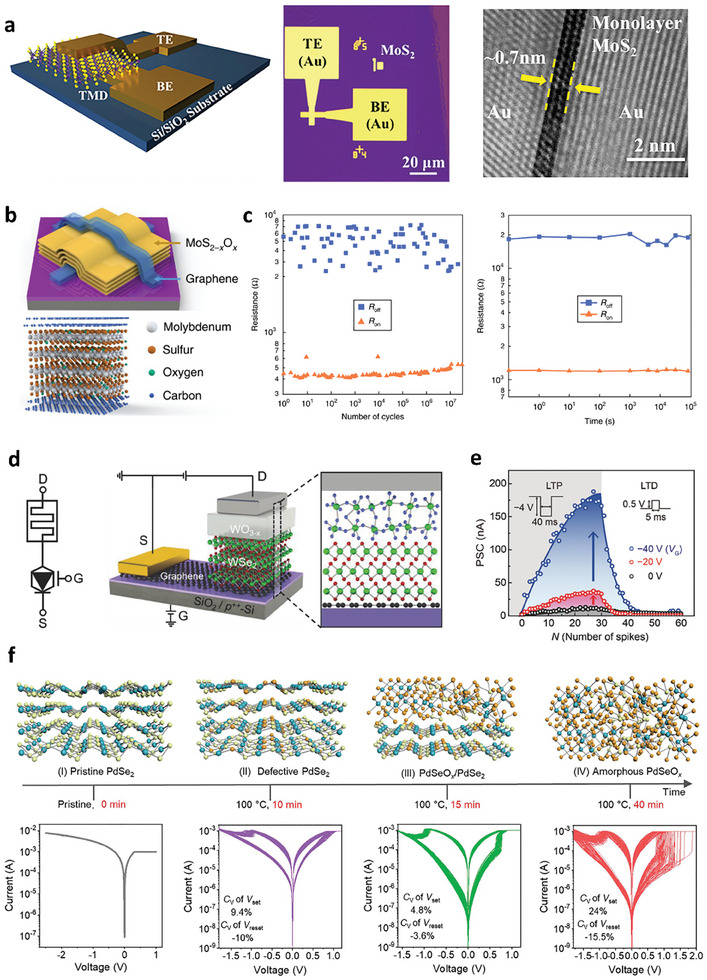
Figure 9.

a) Schematic diagram, OM, and cross‐sectional TEM images for a MoS2 atomic memristor. Reproduced with permission.[ 137 ] Copyright 2018, American Chemistry Society. b,c) Memristor with a graphene/MoS2‐xOx/graphene vertical heterostructure and its endurance and retention characteristics. Reproduced with permission.[ 143 ] Copyright 2018, Springer Nature. d,e) Synaptic barristor fabricated using oxidized TMDs, showing efficient gate‐tunable synaptic behaviors. Reproduced with permission.[ 25 ] Copyright 2018, Wiley‐VCH. f) Controlled resistive switching behaviors for a PdSeOx/PdSe2 heterostructure under different ozone treatment conditions. Reproduced under the terms of the CC‐BY 4.0 license.[ 145 ] Copyright 2022, The Authors, Published by Wiley‐VCH.
