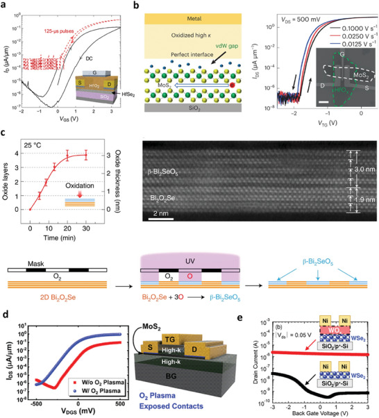
Figure 12.

a) Top‐gated HfSe2 transistor with native HfO2 dielectric. Reproduced under the terms of the CC‐BY‐NC 4.0 license.[ 27 ] Copyright 2017, The Authors, American Association for the Advancement of Science. b) Cross‐sectional representation of the gate interface states in MoS2 VGG transistors. Transfer curves of the VGG transistors with different gate‐voltage sweeping speeds. Reproduced with permission.[ 93 ] Copyright 2022, Springer Nature. c) Layer‐by‐layer oxidation of 2D Bi2O2Se under vacuum‐UV (185 nm) exposure at room temperature. Cross‐sectional STEM‐HAADF image of a uniform ultrathin lattice‐matched single‐crystalline 2D Bi2O2Se/β‐Bi2SeO5 heterostructure. Area‐selective oxidation with UV and photolithography mask free of polymers. Reproduced with permission.[ 171 ] Copyright 2022, Springer Nature. d) Graphic cross section of a dual‐gate (DG) MoS2 FET with a HfO2/Al2O3/MoS2/Al2O3 gate stack. Comparison of transfer curves of DG MoS2 FETs demonstrating a similar, near‐ideal SS of ∼60 mV/dec with over an order of magnitude increase in the ON current for devices with O2 plasma exposure at the contacts. Reproduced with permission.[ 77 ] Copyright 2019, American Chemistry Society. e) I d –V g characteristics of WSe2 FETs with and without a buffered‐WOx layer. Reproduced under the terms of the CC‐BY 4.0 license.[ 175 ] Copyright 2023, The Authors, Published by IEEE.
